
Information


© 2008 Microchip Technology Inc. DS80310G-page 17
PIC18F2221/2321/4221/4321
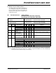
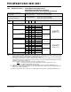
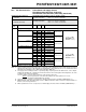
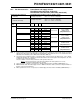
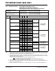
Supply Current (IDD)
(2)
PIC18LF2X21/4X21 160 230 μA-40°C
V
DD = 2.0V
F
OSC = 1 MHz
(RC_IDLE mode,
INTOSC source)
170 230 μA+25°C
170 230 μA+85°C
PIC18LF2X21/4X21 220 330 μA-40°C
VDD = 3.0V240 330 μA+25°C
250 330 μA+85°C
All devices 410 500 μA-40°C
V
DD = 5.0V
420 500 μA+25°C
430 500 μA+85°C
Extended devices only 450 500 μA +125°C
PIC18LF2X21/4X21 310 440 μA-40°C
V
DD = 2.0V
F
OSC = 4 MHz
(RC_IDLE mode,
INTOSC source)
330 440 μA+25°C
340 440 μA+85°C
PIC18LF2X21/4X21 480 750 μA-40°C
VDD = 3.0V500 750 μA+25°C
520 750 μA+85°C
All devices 0.91 1.3 mA -40°C
V
DD = 5.0V
0.93 1.3 mA +25°C
0.96 1.3 mA +85°C
Extended devices only 0.98 1.3 mA +125°C
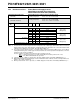
26.2 DC Characteristics: Power-Down and Supply Current
PIC18F2221/2321/4221/4321 (Industrial)
PIC18LF2221/2321/4221/4321 (Industrial) (Continued)
PIC18LF2221/2321/4221/4321
(Industrial)
Standard Operating Conditions (unless otherwise stated)
Operating temperature -40°C ≤ T
A ≤ +85°C for industrial
PIC18F2221/2321/4221/4321
(Industrial, Extended)
Standard Operating Conditions (unless otherwise stated)
Operating temperature -40°C ≤ T
A ≤ +85°C for industrial
-40°C ≤ T
A ≤ +125°C for extended
Param
No.
Device Typ Max Units Conditions
Legend: Shading of rows is to assist in readability of the table.
Note 1: The power-down current in Sleep mode does not depend on the oscillator type. Power-down current is measured
with the part in Sleep mode, with all I/O pins in high-impedance state and tied to VDD or VSS and all features that
add delta current disabled (such as WDT, Timer1 Oscillator, BOR, etc.).
2: The supply current is mainly a function of operating voltage, frequency and mode. Other factors, such as I/O pin
loading and switching rate, oscillator type and circuit, internal code execution pattern and temperature, also have
an impact on the current consumption.
The test conditions for all I
DD measurements in active operation mode are:
OSC1 = external square wave, from rail-to-rail; all I/O pins tri-stated, pulled to V
DD or VSS;
MCLR
= VDD; WDT enabled/disabled as specified.
3: Low-power, Timer1 oscillator is selected unless otherwise indicated, where LPT1OSC (CONFIG3H<2>) =
1.
4: BOR and HLVD enable internal band gap reference. With both modules enabled, current consumption will be less
than the sum of both specifications.
5: When operation below -10°C is expected, use T1OSC high-power mode where LPT1OSC (CONFIG3H<2>) =
0.