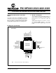
PIC18F2221/2321/4221/4321 PIC18F2221/2321/4221/4321 Data Sheet Errata 1. Module: Pin Diagrams Clarifications/Corrections to the Data Sheet: The pin diagram for the 44-pin TQFP package, on Page 4, has been modified to change the designation for Pins 12, 13, 33 and 34 to “NC”, No Connect. In the Device Data Sheet (DS39689E), the following clarifications and corrections should be noted. Any silicon issues related to the PIC18F2221/2321/4221/4321 will be reported in a separate silicon errata.
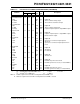
PIC18F2221/2321/4221/4321 2. Module: PIC18F4221/4321 Pinout I/O Descriptions Table 3. Module: PIC18F4221/4321 Pinout I/O Descriptions Table Table 1-3: PIC18F4221/4321 Pinout I/O Descriptions, beginning on Page 16, has been changed to remove Note 3, concerning “Special ICPORT features.” TABLE 1-3: Table 1-3: PIC18F4221/4321 Pinout I/O Descriptions, beginning on Page 16, has been changed to remove four rows. With Data Sheet Clarifications 2 and 3, the table now appears as shown.
PIC18F2221/2321/4221/4321 TABLE 1-3: PIC18F4221/4321 PINOUT I/O DESCRIPTIONS (CONTINUED) Pin Number Pin Name PDIP Pin Buffer Type Type QFN TQFP Description PORTA is a bidirectional I/O port. RA0/AN0 RA0 AN0 2 RA1/AN1 RA1 AN1 3 RA2/AN2/VREF-/CVREF RA2 AN2 VREFCVREF 4 RA3/AN3/VREF+ RA3 AN3 VREF+ 5 RA4/T0CKI/C1OUT RA4 T0CKI C1OUT 6 RA5/AN4/SS/HLVDIN/ C2OUT RA5 AN4 SS HLVDIN C2OUT 7 19 20 21 22 23 24 19 I/O I TTL Analog Digital I/O. Analog input 0. I/O I TTL Analog Digital I/O.
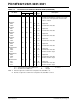
PIC18F2221/2321/4221/4321 TABLE 1-3: PIC18F4221/4321 PINOUT I/O DESCRIPTIONS (CONTINUED) Pin Number Pin Name PDIP Pin Buffer Type Type QFN TQFP Description PORTB is a bidirectional I/O port. PORTB can be software programmed for internal weak pull-ups on all inputs.
PIC18F2221/2321/4221/4321 TABLE 1-3: PIC18F4221/4321 PINOUT I/O DESCRIPTIONS (CONTINUED) Pin Number Pin Name PDIP Pin Buffer Type Type QFN TQFP Description PORTC is a bidirectional I/O port. RC0/T1OSO/T13CKI RC0 T1OSO T13CKI 15 RC1/T1OSI/CCP2 RC1 T1OSI CCP2(1) 16 RC2/CCP1/P1A RC2 CCP1 P1A 17 RC3/SCK/SCL RC3 SCK 18 34 35 36 37 32 23 RC5/SDO RC5 SDO 24 RC6/TX/CK RC6 TX CK 25 RC7/RX/DT RC7 RX DT 26 42 43 44 1 ST — ST Digital I/O. Timer1 oscillator analog output.
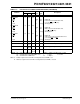
PIC18F2221/2321/4221/4321 TABLE 1-3: PIC18F4221/4321 PINOUT I/O DESCRIPTIONS (CONTINUED) Pin Number Pin Name PDIP Pin Buffer Type Type QFN TQFP Description PORTD is a bidirectional I/O port or a Parallel Slave Port (PSP) for interfacing to a microprocessor port. These pins have TTL input buffers when the PSP module is enabled.
PIC18F2221/2321/4221/4321 TABLE 1-3: PIC18F4221/4321 PINOUT I/O DESCRIPTIONS (CONTINUED) Pin Number Pin Name PDIP Pin Buffer Type Type QFN TQFP Description PORTE is a bidirectional I/O port. RE0/RD/AN5 RE0 RD 8 25 25 AN5 RE1/WR/AN6 RE1 WR 9 26 10 27 — I Analog I/O I ST TTL I Analog I/O I ST TTL I Analog Digital I/O. Read control for Parallel Slave Port (see also WR and CS pins). Analog input 5. Digital I/O. Write control for Parallel Slave Port (see CS and RD pins). Analog input 6.
PIC18F2221/2321/4221/4321 4. Module: Configuration Bits and Device IDs Table 23-1: Configuration Bits and Device IDs, on Page 253, has been changed to designate Bit 3 of CONFIG4L as unimplemented. The table is changed as shown.
PIC18F2221/2321/4221/4321 5. Module: CONFIG4L Register Register 23-5: CONFIG4L: Configuration Register 4 Low (Byte Address 300006h), on Page 258, has been changed to designate Bit 3 of CONFIG4L as unimplemented. The register is changed as shown.
PIC18F2221/2321/4221/4321 6. Module: “Special ICPORT Features” Section Section 23.9 “Special ICPORT Features (44-Pin TQFP Packages Only)” has been removed. That section includes Table 23-5: Equivalent Pins for Legacy and Dedicated ICD/ICSP™ Ports, Section 23.9.1 “Dedicated ICD/ICSP Port” and Section 23.9.2 “28-Pin Emulation” on Pages 271 and 272. 8.
PIC18F2221/2321/4221/4321 9. Module: EUSART In this document’s Revision E change, the Synchronous mode content was removed from the bit 5 (RXDTP) description. The descriptions of the RXDTP and TXCKP bits (BAUDCON<5:4>) are being revised as shown below (changes in bold).
PIC18F2221/2321/4221/4321 10. Module: Packaging Information The 28-Lead Plastic Quad Flat, No Lead Package (MM) illustration, on page 371, is replaced by the one shown. 28-Lead Plastic Quad Flat, No Lead Package (ML) – 6x6 mm Body [QFN] with 0.55 mm Contact Length Note: For the most current package drawings, please see the Microchip Packaging Specification located at http://www.microchip.
PIC18F2221/2321/4221/4321 11. Module: Electrical Characteristics The Supply Voltage, Power-Down and Supply Current, and High/Low-Voltage Detect Characteristics tables are updated as shown. The three tables are reprinted in their entirety, with the updated values indicated by bold text. 26.
PIC18F2221/2321/4221/4321 26.
PIC18F2221/2321/4221/4321 26.
PIC18F2221/2321/4221/4321 26.
PIC18F2221/2321/4221/4321 26.
PIC18F2221/2321/4221/4321 26.
PIC18F2221/2321/4221/4321 26.
PIC18F2221/2321/4221/4321 26.
PIC18F2221/2321/4221/4321 26.
PIC18F2221/2321/4221/4321 26.
PIC18F2221/2321/4221/4321 26.
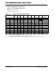
PIC18F2221/2321/4221/4321 TABLE 26-4: HIGH/LOW-VOLTAGE DETECT CHARACTERISTICS Standard Operating Conditions (unless otherwise stated) Operating temperature -40°C ≤ TA ≤ +85°C for industrial Param Symbol No. D420 DS80310G-page 24 Characteristic Min Typ Max Units HLVD Voltage on VDD LVV = 0000 Transition High to Low LVV = 0001 2.06 2.17 2.28 V 2.12 2.23 2.34 V LVV = 0010 2.24 2.36 2.48 V LVV = 0011 2.32 2.44 2.56 V LVV = 0100 2.47 2.60 2.73 V LVV = 0101 2.65 2.79 2.
PIC18F2221/2321/4221/4321 12. Module: Electrical Characteristics (I/O Port Leakage Current) The new values change the first page of Section 26.3 “DC Characteristics” as shown. (New values are indicated by bold text.) The maximum values of the following parameters for input leakage current are changed: • D060 – I/O Ports • D061 – MCLR, RA4 • D063 – OSC1 26.
PIC18F2221/2321/4221/4321 13. Module: Peripheral Highlights 14. Module: A/D Converter Characteristics Under the “Peripheral Highlights” section on page 1, Enhanced Addressable USART module, the first bullet should be changed to: Table 26-24: A/D Converter Characteristics, on page 363, has been changed to update the offset error. The table has been reprinted with the updated values shown in bold text.
PIC18F2221/2321/4221/4321 REVISION HISTORY Rev A Document (3/2007) Original version of this document. Includes Data Sheet Clarifications 1 through 7, removing all ICPORT references from the data sheet. Rev B Document (4/2007) Added Data Sheet Clarification 8 (Product Identification System). Rev C Document (5/2007) Added Data Sheet Clarification 9 (EUSART). Rev D Document (7/2007) Added Data Sheet Clarification Information).
PIC18F2221/2321/4221/4321 NOTES: DS80310G-page 28 © 2008 Microchip Technology Inc.
Note the following details of the code protection feature on Microchip devices: • Microchip products meet the specification contained in their particular Microchip Data Sheet. • Microchip believes that its family of products is one of the most secure families of its kind on the market today, when used in the intended manner and under normal conditions. • There are dishonest and possibly illegal methods used to breach the code protection feature.
WORLDWIDE SALES AND SERVICE AMERICAS ASIA/PACIFIC ASIA/PACIFIC EUROPE Corporate Office 2355 West Chandler Blvd. Chandler, AZ 85224-6199 Tel: 480-792-7200 Fax: 480-792-7277 Technical Support: http://support.microchip.com Web Address: www.microchip.