
Information

2009-2011 Microchip Technology Inc. DS80437F-page 5
PIC18(L)F1XK22
2. Module: ECCP
2.1 Incorrect Dead-Band When Changing
Direction
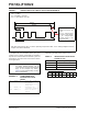
Changing direction in Full-Bridge mode
inserts a dead-band time of 4/F
OSC *TMR2
Prescale instead of 1/F
OSC * TMR2 Prescale
as specified in the data sheet.
Work around
None.
Affected Silicon Revisions
2.2 Dead-Band Ignored When Changing
Direction
In Full-Bridge mode, when PR2 = CCPR1L,
DC1B<1:0> = 00, and the direction is
changed, then the dead time before the mod-
ulated output starts is compromised. The
modulated signal improperly starts immedi-
ately with the direction change and stays on
for T
OSC *TMR2 Prescale* DC1B<1:0>.
Work around
Avoid changing direction when the duty
cycle is within three least significant steps of
100% duty cycle. Instead, clear the
DC1B<1:0> bits before the direction change
and then set them to the desired value after
the direction change is complete.
Affected Silicon Revisions
3. Module: EUSART
3.1 Unreliable RCIDL Bit
In Asynchronous Receive mode, the RCIDL
bit of the BAUDCON register will properly go
low when a low pulse greater than 1/16
th
of
a bit time is received on the RX input. The
RCIDL bit will then improperly go high if a low
pulse less than 1/16 bit time occurs on the
RX input within one bit period, after the fall-
ing edge of the first pulse. This erratum
affects only users monitoring the RCIDL bit
as a part of their serial protocol.
Work around
None.
Affected Silicon Revisions
3.2 OERR Flag Not Cleared as Expected
The OERR flag of the RCSTA register is
reset only by either clearing the CREN bit of
the RCSTA register or by a device Reset.
Clearing the SPEN bit of the RCSTA register
does not clear the OERR flag.
Work around
Clear the OERR flag by clearing the CREN
bit in lieu of clearing the SPEN bit.
Affected Silicon Revisions
3.3 RX and TX are Unavailable for Output
When the SPEN bit of the RCSTA register is
set and the CREN bit of the RCSTA register
is clear, the RX pin is not available for gen-
eral purpose output. Likewise, when the
SPEN bit of the RCSTA register is set and
the TXEN bit of the TXSTA register is clear,
the TX pin is not available for general pur-
pose output. However, both the RX and TX
pins can be read regardless of the state of
the RCSTA and TXSTA control registers.
Work around
None.
Affected Silicon Revisions
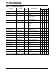
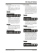
A3 A7 A8 AA
XXX
X
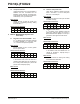
A3 A7 A8 AA
XXX
X
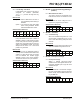
A3 A7 A8 AA
XXX
X
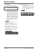
A3 A7 A8
AA
XX
A3 A7 A8 AA
XXX
X