
Information


PIC18(L)F1XK22
DS80437F-page 4 2009-2011 Microchip Technology Inc.
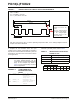
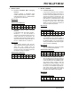
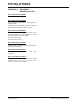
FIGURE 1: INSTRUCTION CYCLE DELAY CALCULATION EXAMPLE
In Figure 1, 88 instruction cycles (TCY) will be required
to complete the full conversion. Each T
AD cycle
consists of 8 T
CY periods. A fixed delay is provided to
stop the A/D conversion after 86 instruction cycles and
terminate the conversion at the correct time as shown
in the figure above.
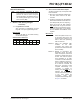
EXAMPLE 1: CODE EXAMPLE OF
INSTRUCTION CYCLE
DELAY
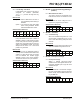
For other combinations of FOSC, TAD values and
Instruction cycle delay counts, refer to Table 3.
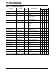
TABLE 3: INSTRUCTION CYCLE DELAY
COUNT VS. T
AD
Affected Silicon Revisions
FOSC = 32 MHz
TCY = 4/32 MHz = 125 nsec
TAD = 1 µsec, ADCS = FOSC/32
88 TCY
84 TCY
8 TCY
4 TCY
1 TAD
11 TAD
Stop the A/D conversion
between 10.5 and 11 T
AD
cycles.
See the Analog-to-Digital
Conversion Timing diagram
in the Analog-to-Digital
Converter chapter of the
device data sheet.
}
See ADC Clock Period (TAD) vs. Device Operating Frequencies Table, in the Analog-to-Digital Converter
chapter of the device data sheet.
Note: The exact delay time will depend on the
T
AD divisor (ADCS) selection. The TCY
counts shown in the timing diagram above
apply to this example only. Refer to
Table 3 for the required delay counts for
other configurations.
BSF ADCON0, GO ; Start ADC conversion
; Provide 86
instruction cycle
delay here
BCF ADCON0, GO ; Terminate the
conversion manually
MOVF ADRESH, W ; Read conversion
result
TAD Instruction Cycle Delay Counts
F
OSC/64 172
FOSC/32 86
FOSC/16 43
A3 A7 A8
AA
XX