
Datasheet


PIC18F1230/1330
2009 Microchip Technology Inc. DS39758D-page 5
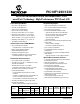
Pin Diagrams (Continued)
28-Pin QFN
(3)
Note 1: Placement of T1OSI and T1OSO/T1CKI depends on the value of Configuration bit, T1OSCMX, of
CONFIG3H.
2: Placement of FLTA
depends on the value of Configuration bit, FLTAMX, of CONFIG3H.
3: It is recommended that the user connect the center metal pad for this device package to the ground.
10 11
2
3
6
1
18
19
20
21
22
12 13 14
15
8
7
16
17
232425262728
9
PIC18F1X30
RA3/RX/DT
5
4
NC
RB3/INT3/KBI3/CMP1/T1OSI
(1)
NC
RA7/OSC1/CLKI/T1OSI
(1)
/FLTA
(2)
VDD
NC
AV
DD
RB7/PWM5/PGD
RB6/PWM4/PGC
NC
RB5/PWM3
RB4/PWM2
RA0/AN0/INT0/KBI0/CMP0
RA1/AN1/INT1/KBI1
RA4/T0CKI/AN2/V
REF+
MCLR/VPP/RA5/FLTA
(2)
NC
V
SS
NC
AV
SS
NC
RA2/TX/CK
RB0/PWM0
RB1/PWM1
NC
RB2/INT2/KBI2/CMP2/T1OSO
(1)
/T1CKI
(1)
RA6/OSC2/CLKO/T1OSO
(1)
/T1CKI
(1)
/AN3