
Datasheet


PIC18F1230/1330
2009 Microchip Technology Inc. DS39758D-page 279
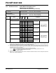
23.3 DC Characteristics: PIC18F1230/1330 (Industrial)
PIC18LF1230/1330 (Industrial)
DC CHARACTERISTICS
Standard Operating Conditions (unless otherwise stated)
Operating temperature -40°C TA +85°C for industrial
-40°C T
A +125°C for extended
Param
No.
Symbol Characteristic Min Max Units Conditions
V
IL Input Low Voltage
I/O ports:
D030 with TTL buffer V
SS 0.15 VDD VVDD < 4.5V
D030A — 0.8 V 4.5V V
DD 5.5V
D031 with Schmitt Trigger buffer VSS 0.2 VDD V
D031A RC3 and RC4 V
SS 0.3 VDD VI
2
C™ enabled
D031B V
SS 0.8 V SMBus enabled
D032 MCLR
VSS 0.2 VDD V
D033 OSC1 VSS 0.3 VDD VHS, HSPLL modes
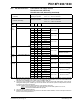
D033A
D033B
D034
OSC1
OSC1
T1CKI
V
SS
VSS
VSS
0.2 VDD
0.3
0.3
V
V
V
RC, EC modes
(1)
XT, LP modes
V
IH Input High Voltage
I/O ports:
D040 with TTL buffer 0.25 VDD + 0.8V VDD VVDD < 4.5V
D040A 2.0 V
DD V4.5V VDD 5.5V
D041 with Schmitt Trigger buffer 0.8 VDD VDD V
D041A RC3 and RC4 0.7 VDD VDD VI
2
C enabled
D041B 2.1 V
DD I
2
C enabled
D042 MCLR
0.8 VDD VDD V
D043 OSC1 0.7 VDD VDD VHS, HSPLL modes
D043A
D043B
D043C
D044
OSC1
OSC1
OSC1
T1CKI
0.8 VDD
0.9 VDD
1.6
1.6
VDD
VDD
VDD
VDD
V
V
V
V
EC mode
RC mode
(1)
XT, LP modes
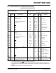
I
IL Input Leakage Current
(2,3)
D060 I/O ports — 200 nA V
SS < 5.5V
Vss V
PIN VDD
Pin at high-impedance
50 nA V
SS < 3V
Vss V
PIN VDD
Pin at high-impedance
D061 MCLR
— 1 AVss VPIN VDD
D063 OSC1 — 1 AVss VPIN VDD
I
PU Weak Pull-up Current
D070 I
PURB PORTB weak pull-up current 50 400 AVDD = 5V, VPIN = VSS
Note 1: In RC oscillator configuration, the OSC1/CLKI pin is a Schmitt Trigger input. It is not recommended that the
PIC
®
device be driven with an external clock while in RC mode.
2: The leakage current on the MCLR pin is strongly dependent on the applied voltage level. The specified
levels represent normal operating conditions. Higher leakage current may be measured at different input
voltages.
3: Negative current is defined as current sourced by the pin.