
Datasheet


PIC18F1230/1330
DS39758D-page 200 2009 Microchip Technology Inc.
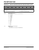
REGISTER 20-11: CONFIG7L: CONFIGURATION REGISTER 7 LOW (BYTE ADDRESS 30000Ch)
U-0 U-0 U-0 U-0 U-0 U-0 R/C-1 R/C-1
— — — — — — EBTR1
(1)
EBTR0
(1)
bit 7 bit 0
Legend:
R = Readable bit C = Clearable bit U = Unimplemented bit, read as ‘0’
-n = Value when device is unprogrammed u = Unchanged from programmed state
bit 7-2 Unimplemented: Read as ‘0’
bit 1 EBTR1: Table Read Protection bit (Block 1 Code Memory Area)
1 = Block 1 is not protected from table reads executed in other blocks
0 = Block 1 is protected from table reads executed in other blocks
bit 0 EBTR0: Table Read Protection bit (Block 0 Code Memory Area)
1 = Block 0 is not protected from table reads executed in other blocks
0 = Block 0 is protected from table reads executed in other blocks
Note 1: It is recommended to enable the corresponding CPx bit to protect block from external read operations.
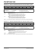
REGISTER 20-12: CONFIG7H: CONFIGURATION REGISTER 7 HIGH (BYTE ADDRESS 30000Dh)
U-0 R/C-1 U-0 U-0 U-0 U-0 U-0 U-0
— EBTRB
(1)
— — — — — —
bit 7 bit 0
Legend:
R = Readable bit C = Clearable bit U = Unimplemented bit, read as ‘0’
-n = Value when device is unprogrammed u = Unchanged from programmed state
bit 7 Unimplemented: Read as ‘0’
bit 6 EBTRB: Table Read Protection bit (Boot Block Memory Area)
1 = Boot Block is not protected from table reads executed in other blocks
0 = Boot Block is protected from table reads executed in other blocks
bit 5-0 Unimplemented: Read as ‘0’
Note 1: It is recommended to enable the corresponding CPx bit to protect block from external read operations.