
Datasheet


PIC18F1230/1330
DS39758D-page 194 2009 Microchip Technology Inc.
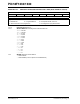
REGISTER 20-3: CONFIG2H: CONFIGURATION REGISTER 2 HIGH (BYTE ADDRESS 300003h)
U-0 U-0 U-0 R/P-1 R/P-1 R/P-1 R/P-1 R/P-1
— — —
WDTPS3 WDTPS2 WDTPS1 WDTPS0 WDTEN
bit 7 bit 0
Legend:
R = Readable bit P = Programmable bit U = Unimplemented bit, read as ‘0’
-n = Value when device is unprogrammed u = Unchanged from programmed state
bit 7-5 Unimplemented: Read as ‘0’
bit 4-1 WDTPS3:WDTPS0: Watchdog Timer Postscale Select bits
1111 = 1:32,768
1110 = 1:16,384
1101 = 1:8,192
1100 = 1:4,096
1011 = 1:2,048
1010 = 1:1,024
1001 = 1:512
1000 = 1:256
0111 = 1:128
0110 = 1:64
0101 = 1:32
0100 = 1:16
0011 = 1:8
0010 = 1:4
0001 = 1:2
0000 = 1:1
bit 0 WDTEN: Watchdog Timer Enable bit
1 = WDT enabled
0 = WDT disabled (control is placed on the SWDTEN bit)