
Datasheet


PIC18F1230/1330
2009 Microchip Technology Inc. DS39758D-page 193
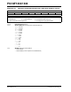
REGISTER 20-2: CONFIG2L: CONFIGURATION REGISTER 2 LOW (BYTE ADDRESS 300002h)
U-0 U-0 U-0 R/P-1 R/P-1 R/P-1 R/P-1 R/P-1
— — —BORV1
(1)
BORV0
(1)
BOREN1
(2)
BOREN0
(2)
PWRTEN
(2)
bit 7 bit 0
Legend:
R = Readable bit P = Programmable bit U = Unimplemented bit, read as ‘0’
-n = Value when device is unprogrammed u = Unchanged from programmed state
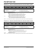
bit 7-5 Unimplemented: Read as ‘0’
bit 4-3 BORV1:BORV0: Brown-out Reset Voltage bits
(1)
11 = Minimum setting
•
•
•
00 = Maximum setting
bit 2-1 BOREN1:BOREN0: Brown-out Reset Enable bits
(2)
11 = Brown-out Reset enabled in hardware only (SBOREN is disabled)
10 = Brown-out Reset enabled in hardware only and disabled in Sleep mode (SBOREN is disabled)
01 = Brown-out Reset enabled and controlled by software (SBOREN is enabled)
00 = Brown-out Reset disabled in hardware and software
bit 0 PWRTEN
: Power-up Timer Enable bit
(2)
1 = PWRT disabled
0 = PWRT enabled
Note 1: See Section 23.1 “DC Characteristics” for the specifications.
2: The Power-up Timer is decoupled from Brown-out Reset, allowing these features to be independently
controlled.