
Datasheet


2009 Microchip Technology Inc. DS39758D-page 19
PIC18F1230/1330
2.3 Master Clear (MCLR) Pin
The MCLR pin provides two specific device
functions: Device Reset, and Device Programming
and Debugging. If programming and debugging are
not required in the end application, a direct
connection to V
DD may be all that is required. The
addition of other components, to help increase the
application’s resistance to spurious Resets from
voltage sags, may be beneficial. A typical
configuration is shown in Figure 2-1. Other circuit
designs may be implemented, depending on the
application’s requirements.
During programming and debugging, the resistance
and capacitance that can be added to the pin must be
considered. Device programmers and debuggers drive
the MCLR
pin. Consequently, specific voltage levels
(V
IH and VIL) and fast signal transitions must not be
adversely affected. Therefore, specific values of R1
and C1 will need to be adjusted based on the
application and PCB requirements. For example, it is
recommended that the capacitor, C1, be isolated from
the MCLR
pin during programming and debugging
operations by using a jumper (Figure 2-2). The jumper
is replaced for normal run-time operations.
Any components associated with the MCLR
pin
should be placed within 0.25 inch (6 mm) of the pin.
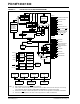
FIGURE 2-2: EXAMPLE OF MCLR PIN
CONNECTIONS
2.4 ICSP Pins
The PGC and PGD pins are used for In-Circuit Serial
Programming™ (ICSP™) and debugging purposes. It
is recommended to keep the trace length between the
ICSP connector and the ICSP pins on the device as
short as possible. If the ICSP connector is expected to
experience an ESD event, a series resistor is recom-
mended, with the value in the range of a few tens of
ohms, not to exceed 100Ω.
Pull-up resistors, series diodes, and capacitors on the
PGC and PGD pins are not recommended as they will
interfere with the programmer/debugger communica-
tions to the device. If such discrete components are an
application requirement, they should be removed from
the circuit during programming and debugging. Alter-
natively, refer to the AC/DC characteristics and timing
requirements information in the respective device
Flash programming specification for information on
capacitive loading limits and pin input voltage high (V
IH)
and input low (V
IL) requirements.
For device emulation, ensure that the “Communication
Channel Select” (i.e., PGCx/PGDx pins) programmed
into the device matches the physical connections for
the ICSP to the Microchip debugger/emulator tool.
For more information on available Microchip
development tools connection requirements, refer to
Section 21.0 “Development Support”.
Note 1: R1 10 k is recommended. A suggested
starting value is 10 k. Ensure that the
MCLR
pin VIH and VIL specifications are met.
2: R2 470 will limit any current flowing into
MCLR
from the external capacitor, C, in the
event of MCLR
pin breakdown, due to
Electrostatic Discharge (ESD) or Electrical
Overstress (EOS). Ensure that the MCLR
pin
V
IH and VIL specifications are met.
C1
R2
R1
V
DD
MCLR
PIC18FXXXX
JP