
Datasheet


PIC18F1230/1330
2009 Microchip Technology Inc. DS39758D-page 161
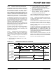
FIGURE 15-7: ASYNCHRONOUS RECEPTION
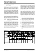
TABLE 15-6: REGISTERS ASSOCIATED WITH ASYNCHRONOUS RECEPTION
15.2.4 AUTO-WAKE-UP ON SYNC
BREAK CHARACTER
During Sleep mode, all clocks to the EUSART are
suspended. Because of this, the Baud Rate Generator
is inactive and a proper byte reception cannot be
performed. The auto-wake-up feature allows the
controller to wake-up due to activity on the RX/DT line
while the EUSART is operating in Asynchronous mode.
The auto-wake-up feature is enabled by setting the
WUE bit (BAUDCON<1>). Once set, the typical receive
sequence on RX/DT is disabled and the EUSART
remains in an Idle state, monitoring for a wake-up event
independent of the CPU mode. A wake-up event
consists of a high-to-low transition on the RX/DT line.
(This coincides with the start of a Sync Break or a
Wake-up Signal character for the LIN/J2602 protocol.)
Following a wake-up event, the module generates an
RCIF interrupt. The interrupt is generated
synchronously to the Q clocks in normal operating
modes (Figure 15-8) and asynchronously if the device
is in Sleep mode (Figure 15-9). The interrupt condition
is cleared by reading the RCREG register.
The WUE bit is automatically cleared once a low-to-
high transition is observed on the RX line following the
wake-up event. At this point, the EUSART module is in
Idle mode and returns to normal operation. This signals
to the user that the Sync Break event is over.
Name Bit 7 Bit 6 Bit 5 Bit 4 Bit 3 Bit 2 Bit 1 Bit 0
Reset
Values
on Page:
INTCON GIE/GIEH PEIE/GIEL
TMR0IE INT0IE RBIE TMR0IF INT0IF RBIF 47
PIR1 — ADIF RCIF TXIF CMP2IF CMP1IF CMP0IF TMR1IF 49
PIE1 — ADIE RCIE TXIE CMP2IE CMP1IE CMP0IE TMR1IE 49
IPR1
— ADIP RCIP TXIP CMP2IP CMP1IP CMP0IP TMR1IP 49
RCSTA SPEN RX9 SREN CREN ADDEN FERR OERR RX9D 48
RCREG EUSART Receive Register 48
TXSTA
CSRC TX9 TXEN SYNC SENDB BRGH TRMT TX9D 48
BAUDCON ABDOVF RCIDL RXDTP TXCKP BRG16 — WUE ABDEN 48
SPBRGH EUSART Baud Rate Generator Register High Byte 48
SPBRG EUSART Baud Rate Generator Register Low Byte 48
Legend: — = unimplemented locations read as ‘0’. Shaded cells are not used for asynchronous reception.
Start
bit
bit 7/8
bit 1bit 0 bit 7/8
bit 0
Stop
bit
Start
bit
Start
bit
bit 7/8
Stop
bit
RX (pin)
Rcv Buffer Reg
Rcv Shift Reg
Read Rcv
Buffer Reg
RCREG
RCIF
(Interrupt Flag)
OERR bit
CREN
Word 1
RCREG
Word 2
RCREG
Stop
bit
Note: This timing diagram shows three words appearing on the RX input. The RCREG (Receive Buffer) is read after the third word causing
the OERR (Overrun) bit to be set.