
Datasheet


PIC18F1230/1330
DS39758D-page 140 2009 Microchip Technology Inc.
14.10.3 OUTPUT OVERRIDE EXAMPLES
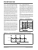
Figure 14-21 shows an example of a waveform that
might be generated using the PWM output override
feature. The figure shows a six-step commutation
sequence for a BLDC motor. The motor is driven
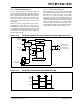
through a 3-phase inverter as shown in Figure 14-16.
When the appropriate rotor position is detected, the
PWM outputs are switched to the next commutation
state in the sequence. In this example, the PWM
outputs are driven to specific logic states. The
OVDCOND and OVDCONS register values used to
generate the signals in Figure 14-21 are given in
Table 14-4.
The PWM Duty Cycle registers may be used in
conjunction with the OVDCOND and OVDCONS
registers. The Duty Cycle registers control the average
voltage across the load and the OVDCOND and
OVDCONS registers control the commutation
sequence. Figure 14-22 shows the waveforms, while
Table 14-4 and Table 14-5 show the OVDCOND and
OVDCONS register values used to generate the
signals.
REGISTER 14-6: OVDCOND: OUTPUT OVERRIDE CONTROL REGISTER
U-0 U-0 R/W-1 R/W-1 R/W-1 R/W-1 R/W-1 R/W-1
— — POVD5 POVD4 POVD3 POVD2 POVD1 POVD0
bit 7 bit 0
Legend:
R = Readable bit W = Writable bit U = Unimplemented bit, read as ‘0’
-n = Value at POR ‘1’ = Bit is set ‘0’ = Bit is cleared x = Bit is unknown
bit 7-6 Unimplemented: Read as ‘0’
bit 5-0 POVD5:POVD0: PWM Output Override bits
1 = Output on PWM I/O pin is controlled by the value in the Duty Cycle register and the PWM time base
0 = Output on PWM I/O pin is controlled by the value in the corresponding POUTx bit
REGISTER 14-7: OVDCONS: OUTPUT STATE REGISTER
U-0 U-0 R/W-0 R/W-0 R/W-0 R/W-0 R/W-0 R/W-0
— — POUT5 POUT4 POUT3 POUT2 POUT1 POUT0
bit 7 bit 0
Legend:
R = Readable bit W = Writable bit U = Unimplemented bit, read as ‘0’
-n = Value at POR ‘1’ = Bit is set ‘0’ = Bit is cleared x = Bit is unknown
bit 7-6 Unimplemented: Read as ‘0’
bit 5-0 POUT5:POUT0: PWM Manual Output bits
(1)
1 = Output on PWM I/O pin is active when the corresponding PWM output override bit is cleared
0 = Output on PWM I/O pin is inactive when the corresponding PWM output override bit is cleared
Note 1: With PWMs configured in complementary mode, even PWM (PWM0, 2, 4) outputs will be
complementary of the odd PWM (PWM1, 3, 5) outputs, irrespective of the POUT bit
setting.