
Datasheet


PIC18F1230/1330
DS39758D-page 12 2009 Microchip Technology Inc.
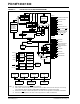
FIGURE 1-1: PIC18F1230/1330 (18-PIN) BLOCK DIAGRAM
Instruction
Decode &
Control
PORTA
RA2/TX/CK
Enhanced
Timer0
Timer1
PCPWM
MCLR/VPP/RA5
(1)
/FLTA
(4)
RA4/T0CKI/AN2/VREF+
RA1/AN1/INT1/KBI1
RA0/AN0/INT0/KBI0/CMP0
Data Latch
Data RAM
Address Latch
Address<12>
12
BSR
FSR0
FSR1
FSR2
4
12 4
PCH PCL
PCLATH
8
31 Level Stack
Program Counter
PRODLPRODH
8 x 8 Multiply
WREG
8
BIT OP
8
8
ALU<8>
8
Address Latch
(8 Kbytes)
Data Latch
20
21
21
16
8
8
8
inc/dec logic
21
8
Data Bus<8>
8
Instruction
12
3
ROM Latch
Bank0, F
PCLATU
PCU
RA3/RX/DT
USART
8
Register
Table Latch
Tab l e P oi n ter < 2>
inc/dec
logic
RB0/PWM0
Decode
Power-up
Timer
Power-on
Reset
Watchdog
Timer
V
DD, VSS
Brown-out
Reset
Precision
Reference
Voltage
Low-Voltage
Programming
In-Circuit
Debugger
Oscillator
Start-up Timer
Timing
Generation
OSC1
(2)
OSC2
(2)
T1OSI
T1OSO
INTRC
Oscillator
Fail-Safe
Clock Monitor
Note 1: RA5 is available only when the MCLR Reset is disabled.
2: OSC1, OSC2, CLKI and CLKO are only available in select oscillator modes and when these pins are not being
used as digital I/O. Refer to Section 3.0 “Oscillator Configurations” for additional information.
3: Placement of T1OSI and T1OSO/T1CKI depends on the value of the Configuration bit, T1OSCMX, of CONFIG3H.
4: Placement of FLTA
depends on the value of the Configuration bit, FLTAMX, of CONFIG3H.
8
Program Memory
(4 Kbytes)
PIC18F1230
PIC18F1330
10-Bit
Data EEPROM
MCLR
(1)
BOR
LVD
A/D Converter
RB1/PWM1
RB7/PWM5/PGD
RA6/OSC2
(2)
/CLKO
(2)
/
RA7/OSC1
(2)
/CLKI
(2)
/
RB2/INT2/KBI2/CMP2/
RB3/INT3/KBI3/CMP1/
RB6/PWM4/PGC
RB5/PWM3
RB4/PWM2
PORTB
T1OSI
(3)
T1OSO
(3)
/T1CKI
(3)
T1OSI
(3)
/FLTA
(4)
T1OSO
(3)
/T1CKI
(3)
/AN3