
Datasheet


PIC18F1230/1330
2009 Microchip Technology Inc. DS39758D-page 113
13.2 Timer1 Oscillator
A crystal oscillator circuit is built-in between pins T1OSI
(input) and T1OSO/TICKI (amplifier output). The place-
ment of these pins depends on the value of Configuration
bit, T1OSCMX (see Section 20.1 “Configuration
Bits”). It is enabled by setting control bit T1OSCEN
(T1CON<3>). The oscillator is a low-power oscillator
rated for 32 kHz crystals. It will continue to run during all
power-managed modes. The circuit for a typical LP
oscillator is shown in Figure 13-3. Table 13-1 shows the
capacitor selection for the Timer1 oscillator.
The user must provide a software time delay to ensure
proper start-up of the Timer1 oscillator.
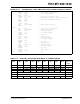
FIGURE 13-3: EXTERNAL
COMPONENTS FOR THE
TIMER1 LP OSCILLATOR
TABLE 13-1: CAPACITOR SELECTION FOR
THE TIMER OSCILLATOR
13.2.1 USING TIMER1 AS A CLOCK
SOURCE
The Timer1 oscillator is also available as a clock source
in power-managed modes. By setting the System
Clock Select bits, SCS1:SCS0 (OSCCON<1:0>), to
‘01’, the device switches to SEC_RUN mode; both the
CPU and peripherals are clocked from the Timer1 oscil-
lator. If the IDLEN bit (OSCCON<7>) is cleared and a
SLEEP instruction is executed, the device enters
SEC_IDLE mode. Additional details are available in
Section 4.0 “Power-Managed Modes”.
Whenever the Timer1 oscillator is providing the clock
source, the Timer1 system clock status flag, T1RUN
(T1CON<6>), is set. This can be used to determine the
controller’s current clocking mode. It can also indicate
the clock source being currently used by the Fail-Safe
Clock Monitor. If the Clock Monitor is enabled and the
Timer1 oscillator fails while providing the clock, polling
the T1RUN bit will indicate whether the clock is being
provided by the Timer1 oscillator or another source.
13.3 Timer1 Oscillator Layout
Considerations
The oscillator circuit, shown in Figure 13-3, should be
located as close as possible to the microcontroller.
There should be no circuits passing within the oscillator
circuit boundaries other than V
SS or VDD.
If a high-speed circuit must be located near the
oscillator (such as the PWM pin, or the primary
oscillator using the OSC2 pin), a grounded guard ring
around the oscillator circuit, as shown in Figure 13-4,
may be helpful when used on a single-sided PCB, or in
addition to a ground plane.
FIGURE 13-4: OSCILLATOR CIRCUIT
WITH GROUNDED GUARD
RING
Osc Type Freq C1 C2
LP 32 kHz 27 pF
(1)
27 pF
(1)
Note 1: Microchip suggests this value as a starting
point in validating the oscillator circuit.
2: Higher capacitance increases the stability
of the oscillator, but also increases the
start-up time.
3: Since each resonator/crystal has its own
characteristics, the user should consult
the resonator/crystal manufacturer for
appropriate values of external
components.
4: Capacitor values are for design guidance
only.
Note: See the notes with Table 13-1 for addi-
tional information about capacitor selec-
C1
C2
XTAL
PIC18FXXXX
T1OSI
T1OSO/T1CKI
32.768 kHz
33 pF
33 pF
RB3
RB2
OSC1
OSC2
V
DD
Note: Not drawn to scale.