
Datasheet


PIC18F1230/1330
2009 Microchip Technology Inc. DS39758D-page 101
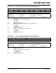
REGISTER 11-8: PIE2: PERIPHERAL INTERRUPT ENABLE REGISTER 2
R/W-0 U-0 U-0 R/W-0 U-0 R/W-0 U-0 U-0
OSCFIE — — EEIE —LVDIE — —
bit 7 bit 0
Legend:
R = Readable bit W = Writable bit U = Unimplemented bit, read as ‘0’
-n = Value at POR ‘1’ = Bit is set ‘0’ = Bit is cleared x = Bit is unknown
bit 7 OSCFIE: Oscillator Fail Interrupt Enable bit
1 = Enabled
0 =Disabled
bit 6-5 Unimplemented: Read as ‘0’
bit 4 EEIE: Data EEPROM/Flash Write Operation Interrupt Enable bit
1 = Enabled
0 =Disabled
bit 3 Unimplemented: Read as ‘0’
bit 2 LVDIE: Low-Voltage Detect Interrupt Enable bit
1 = Enabled
0 =Disabled
bit 1-0 Unimplemented: Read as ‘0’
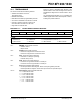
REGISTER 11-9: PIE3: PERIPHERAL INTERRUPT ENABLE REGISTER 3
U-0 U-0 U-0 R/W-0 U-0 U-0 U-0 U-0
— — —PTIE— — — —
bit 7 bit 0
Legend:
R = Readable bit W = Writable bit U = Unimplemented bit, read as ‘0’
-n = Value at POR ‘1’ = Bit is set ‘0’ = Bit is cleared x = Bit is unknown
bit 7-5 Unimplemented: Read as ‘0’
bit 4 PTIE: PWM Time Base Interrupt Enable bit
1 = PWM enabled
0 = PWM disabled
bit 3-0 Unimplemented: Read as ‘0’