
Datasheet


PIC18F1230/1330
2009 Microchip Technology Inc. DS39758D-page 207
20.5 Program Verification and
Code Protection
The overall structure of the code protection on the
PIC18 Flash devices differs significantly from other
PIC
®
devices.
The user program memory is divided into three blocks.
One of these is a Boot Block of variable size (maximum
2 Kbytes). The remainder of the memory is divided into
two blocks on binary boundaries.
Each of the three blocks has three code protection bits
associated with them. They are:
• Code-Protect bit (CPx)
• Write-Protect bit (WRTx)
• External Block Table Read bit (EBTRx)
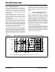
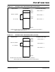
Figure 20-5 shows the program memory organization
for 4 and 8-Kbyte devices and the specific code
protection bit associated with each block. The actual
locations of the bits are summarized in Table 20-3.
FIGURE 20-5: CODE-PROTECTED PROGRAM MEMORY FOR PIC18F1230/1330
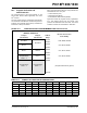
TABLE 20-3: SUMMARY OF CODE PROTECTION REGISTERS
File Name Bit 7 Bit 6 Bit 5 Bit 4 Bit 3 Bit 2 Bit 1 Bit 0
300008h CONFIG5L — — — — — —CP1CP0
300009h CONFIG5H CPD CPB — — — — — —
30000Ah CONFIG6L — — — — — —WRT1WRT0
30000Bh CONFIG6H WRTD WRTB
WRTC — — — — —
30000Ch CONFIG7L
— — — — — — EBTR1 EBTR0
30000Dh CONFIG7H
— EBTRB — — — — — —
Legend: Shaded cells are unimplemented.
MEMORY SIZE/DEVICE
Block Code Protection
Controlled By:
4Kbytes
(PIC18F1230)
8Kbytes
(PIC18F1330)
Address
Range
Boot Block
Boot Block
000000h
0003FFh
CPB, WRTB, EBTRB
Block 0
000400h
0007FFh
CP0, WRT0, EBTR0
Block 1 Block 0
000800h
000FFFh
CP1, WRT1, EBTR1
Unimplemented
Read ‘0’s
Block 1
001000h
001FFFh
CP2, WRT2, EBTR2
Unimplemented
Read ‘0’s
Unimplemented
Read ‘0’s
002000h
1FFFFFh
(Unimplemented Memory Space)