
Datasheet


PIC18F1230/1330
2009 Microchip Technology Inc. DS39758D-page 119
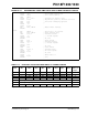
FIGURE 14-2: PWM MODULE BLOCK DIAGRAM, ONE OUTPUT PAIR, COMPLEMENTARY MODE
FIGURE 14-3: PWM MODULE BLOCK DIAGRAM, ONE OUTPUT PAIR, INDEPENDENT MODE
This module contains three duty cycle generators,
numbered 0 through 2. The module has six PWM
output pins, numbered 0 through 5. The six PWM
outputs are grouped into output pairs of even and odd
numbered outputs. In Complementary modes, the
even PWM pins must always be the complement of the
corresponding odd PWM pins. For example, PWM0 will
be the complement of PWM1 and PWM2 will be the
complement of PWM3. The dead-time generator
inserts an OFF period called “dead time” between the
going OFF of one pin to the going ON of the
complementary pin of the paired pins. This is to prevent
damage to the power switching devices that will be
connected to the PWM output pins.
The time base for the PWM module is provided by its
own 12-bit timer, which also incorporates selectable
prescaler and postscaler options.
PWM Duty Cycle Register
Duty Cycle Comparator
Dead-Band
Generator
Fault Override Values
Channel Override Values
Fault Pin Assignment
Logic
Fault A pin
HPOL
LPOL
PWM1
PWM0
VDD
Note: In the Complementary mode, the even channel cannot be forced active by a Fault or override event when the odd channel is
active. The even channel is always the complement of the odd channel and is inactive, with dead time inserted, before the odd
channel is driven to its active state.
Duty Cycle Comparator
PWM Duty Cycle Register
Fault A pin
HPOL
LPOL
PWM1
PWM0
VDD
VDD
Fault Override Values
Channel Override Values
Fault Pin Assignment
Logic