
Datasheet


PIC18F1230/1330
2009 Microchip Technology Inc. DS39758D-page 91
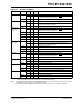
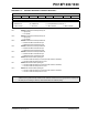
TABLE 10-3: PORTB I/O SUMMARY
Pin Function
TRIS
Setting
I/O
I/O
Type
Description
RB0/PWM0 RB0 0 O DIG LATB<0> data output; not affected by analog input.
1 I TTL PORTB<0> data input; weak pull-up when RBPU
bit is cleared.
Disabled when analog input enabled.
(1)
PWM0 0 O DIG PWM module output PWM0.
RB1PWM1 RB1 0 O DIG LATB<1> data output; not affected by analog input.
1 I TTL PORTB<1> data input; weak pull-up when RBPU
bit is cleared.
Disabled when analog input enabled.
(1)
PWM1 0 O DIG PWM module output PWM1.
RB2/INT2/KBI2/
CMP2/T1OSO/
T1CKI
RB2 0 O DIG LATB<2> data output; not affected by analog input.
1 I TTL PORTB<2> data input; weak pull-up when RBPU
bit is cleared.
Disabled when analog input enabled.
(1)
INT2 1 I ST External interrupt 2 input.
KBI2 1 I TTL Interrupt-on-change pin.
CMP2 1 I ANA Comparator 2 input.
T1OSO
(2)
0 O ANA Timer1 oscillator output.
T1CKI
(2)
1 I ST Timer1 clock input.
RB3/INT3/KBI3/
CMP1/T1OSI
RB3 0 O DIG LATB<3> data output; not affected by analog input.
1 I TTL PORTB<3> data input; weak pull-up when RBPU
bit is cleared.
Disabled when analog input enabled.
(1)
INT3 1 I ST External interrupt 3 input.
KBI3 1 I TTL Interrupt-on-change pin.
CMP1 1 I ANA Comparator 1 input.
T1OSI
(2)
1 I ANA Timer1 oscillator input.
RB4/PWM2 RB4 0 O DIG LATB<4> data output; not affected by analog input.
1 I TTL PORTB<4> data input; weak pull-up when RBPU
bit is cleared.
Disabled when analog input enabled.
(1)
PWM2 0 O DIG PWM module output PWM2.
RB5/PWM3 RB5 0 O DIG LATB<5> data output.
1 I TTL PORTB<5> data input; weak pull-up when RBPU
bit is cleared.
PWM3 0 O DIG PWM module output PWM3.
RB6/PWM4/PGC RB6 0 O DIG LATB<6> data output.
1 I TTL PORTB<6> data input; weak pull-up when RBPU
bit is cleared.
PWM4 0 O DIG PWM module output PWM4.
PGC 1 I ST In-Circuit Debugger and ICSP™ programming clock pin.
RB7/PWM5/PGD RB7 0 O DIG LATB<7> data output.
1 I TTL PORTB<7> data input; weak pull-up when RBPU
bit is cleared.
PWM5 0 O TTL PWM module output PWM4.
PGD 0 O DIG In-Circuit Debugger and ICSP programming data pin.
Legend: DIG = Digital level output; TTL = TTL input buffer; ST = Schmitt Trigger input buffer; ANA = Analog level input/output;
x = Don’t care (TRIS bit does not affect port direction or is overridden for this option).
Note 1: Configuration on POR is determined by the PBADEN Configuration bit. Pins are configured as analog inputs by default
when PBADEN is set and digital inputs when PBADEN is cleared.
2: Placement of T1OSI and T1OSO/T1CKI depends on the value of Configuration bit, T1OSCMX, of CONFIG3H.