
Datasheet


PIC18F1230/1330
2009 Microchip Technology Inc. DS39758D-page 9
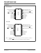
1.0 DEVICE OVERVIEW
This document contains device-specific information for
the following devices:
This family offers the advantages of all PIC18 micro-
controllers – namely, high computational performance at
an economical price – with the addition of high-
endurance Enhanced Flash program memory. On top of
these features, the PIC18F1230/1330 family introduces
design enhancements that make these microcontrollers
a logical choice for many high-performance, power
control and motor control applications.
Peripheral highlights include:
• 14-bit resolution Power Control PWM module
(PCPWM) with programmable dead-time insertion
The PCPWM can generate up to six complementary
PWM outputs with dead-band time insertion. Overdrive
current is detected by off-chip analog comparators or
the digital Fault input (FLTA
).
PIC18F1230/1330 devices also feature Flash program
memory and an internal RC oscillator.
1.1 New Core Features
1.1.1 nanoWatt TECHNOLOGY
All of the devices in the PIC18F1230/1330 family incor-
porate a range of features that can significantly reduce
power consumption during operation. Key items
include:
• Alternate Run Modes: By clocking the controller
from the Timer1 source or the internal oscillator
block, power consumption during code execution
can be reduced by as much as 90%.
• Multiple Idle Modes: The controller can also run
with its CPU core disabled but the peripherals still
active. In these states, power consumption can be
reduced even further, to as little as 4% of normal
operation requirements.
• On-the-Fly Mode Switching: The power-managed
modes are invoked by user code during operation,
allowing the user to incorporate power-saving ideas
into their application’s software design.
• Low Consumption in Key Modules: The power
requirements for both Timer1 and the Watchdog
Timer are minimized. See Section 23.0 “Electrical
Characteristics” for values.
1.1.2 MULTIPLE OSCILLATOR OPTIONS
AND FEATURES
All of the devices in the PIC18F1230/1330 family offer
ten different oscillator options, allowing users a wide
range of choices in developing application hardware.
These include:
• Four Crystal modes, using crystals or ceramic
resonators.
• Two External Clock modes, offering the option of
using two pins (oscillator input and a divide-by-4
clock output) or one pin (oscillator input, with the
second pin reassigned as general I/O).
• Two External RC Oscillator modes with the same
pin options as the External Clock modes.
• An internal oscillator block which provides an 8 MHz
clock and an INTRC source (approximately 31 kHz),
as well as a range of six user-selectable clock
frequencies, between 125 kHz to 4 MHz, for a total of
eight clock frequencies. This option frees the two
oscillator pins for use as additional general
purpose I/Os.
• A Phase Lock Loop (PLL) frequency multiplier,
available to both the High-Speed Crystal and Internal
Oscillator modes, which allows clock speeds of up to
40 MHz. Used with the internal oscillator, the PLL
gives users a complete selection of clock speeds,
from 31 kHz to 32 MHz, all without using an external
crystal or clock circuit.
Besides its availability as a clock source, the internal
oscillator block provides a stable reference source that
gives the family additional features for robust
operation:
• Fail-Safe Clock Monitor: This option constantly
monitors the main clock source against a reference
signal provided by the internal oscillator. If a clock
failure occurs, the controller is switched to the
internal oscillator block, allowing for continued
low-speed operation or a safe application
shutdown.
• Two-Speed Start-up: This option allows the
internal oscillator to serve as the clock source
from Power-on Reset, or wake-up from Sleep
mode, until the primary clock source is available.
• PIC18F1230 • PIC18F1330
• PIC18LF1230 • PIC18LF1330