
Datasheet


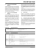


PIC18F1230/1330
DS39758D-page 82 2009 Microchip Technology Inc.
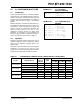
REGISTER 8-1: EECON1: EEPROM CONTROL REGISTER 1
R/W-x R/W-x U-0 R/W-0 R/W-x R/W-0 R/S-0 R/S-0
EEPGD CFGS — FREE WRERR
(1)
WREN WR RD
bit 7 bit 0
Legend: S = Settable bit
R = Readable bit W = Writable bit U = Unimplemented bit, read as ‘0’
-n = Value at POR ‘1’ = Bit is set ‘0’ = Bit is cleared x = Bit is unknown
bit 7 EEPGD: Flash Program or Data EEPROM Memory Select bit
1 = Access Flash program memory
0 = Access data EEPROM memory
bit 6 CFGS: Flash Program/Data EEPROM or Configuration Select bit
1 = Access Configuration registers
0 = Access Flash program or data EEPROM memory
bit 5 Unimplemented: Read as ‘0’
bit 4 FREE: Flash Row Erase Enable bit
1 = Erase the program memory row addressed by TBLPTR on the next WR command
(cleared by completion of erase operation)
0 = Perform write-only
bit 3 WRERR: EEPROM Error Flag bit
(1)
1 = A write operation is prematurely terminated
(MCLR
or WDT Reset during self-timed erase or program operation)
0 = The write operation completed
bit 2 WREN: Erase/Write Enable bit
1 = Allows erase/write cycles
0 = Inhibits erase/write cycles
bit 1 WR: Write Control bit
1 = Initiates a data EEPROM erase/write cycle or a program memory erase cycle or write cycle.
(The operation is self-timed and the bit is cleared by hardware once write is complete.
The WR bit can only be set (not cleared) in software.)
0 = Write cycle to is completed
bit 0 RD: Read Control bit
1 = Initiates a memory read. (Read takes one cycle. RD is cleared in hardware. The RD bit can only be
set (not cleared) in software. RD bit cannot be set when EEPGD = 1.)
0 = Read completed
Note 1: When a WRERR occurs, the EEPGD or FREE bit is not cleared. This allows tracing of the error condition.