
Datasheet


PIC18F1230/1330
2009 Microchip Technology Inc. DS39758D-page 269
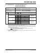
23.2 DC Characteristics: Power-Down and Supply Current
PIC18F1230/1330 (Industrial)
PIC18LF1230/1330 (Industrial)
PIC18LF1230/1330
(Industrial)
Standard Operating Conditions (unless otherwise stated)
Operating temperature -40°C T
A +85°C for industrial
PIC18F1230/1330
(Industrial, Extended)
Standard Operating Conditions (unless otherwise stated)
Operating temperature -40°C T
A +85°C for industrial
-40°C T
A +125°C for extended
Param
No.
Device Typ Max Units Conditions
Power-Down Current (I
PD)
(1)
PIC18LF1230/1330 100 742 nA -40°C
V
DD = 2.0V
(Sleep mode)
0.1 0.742 A+25°C
0.2 4.80 A+85°C
PIC18LF1230/1330 0.1 1.20 A-40°C
V
DD = 3.0V
(Sleep mode)
0.1 1.20 A+25°C
0.3 7.80 A+85°C
All devices 0.1 7.79 A-40°C
V
DD = 5.0V
(Sleep mode)
0.1 7.79 A+25°C
0.4 14.8 A+85°C
Extended devices only 10 119 A +125°C
Note 1: The power-down current in Sleep mode does not depend on the oscillator type. Power-down current is measured
with the part in Sleep mode, with all I/O pins in high-impedance state and tied to V
DD or VSS and all features that
add delta current disabled (such as WDT, Timer1 oscillator, BOR, etc.).
2: The supply current is mainly a function of operating voltage, frequency and mode. Other factors, such as I/O pin
loading and switching rate, oscillator type and circuit, internal code execution pattern and temperature, also have
an impact on the current consumption.
The test conditions for all I
DD measurements in active operation mode are:
OSC1 = external square wave, from rail-to-rail; all I/O pins tri-stated, pulled to V
DD or VSS;
MCLR
= VDD; WDT enabled/disabled as specified.
3: Low-power Timer1 oscillator selected.
4: BOR and LVD enable internal band gap reference. With both modules enabled, current consumption will be less
than the sum of both specifications.