
Datasheet


PIC18F1230/1330
DS39758D-page 268 2009 Microchip Technology Inc.
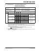
23.1 DC Characteristics: Supply Voltage
PIC18F1230/1330 (Industrial)
PIC18LF1230/1330 (Industrial)
PIC18LF1230/1330
(Industrial)
Standard Operating Conditions (unless otherwise stated)
Operating temperature -40°C T
A +85°C for industrial
PIC18F1230/1330
(Industrial, Extended)
Standard Operating Conditions (unless otherwise stated)
Operating temperature -40°C T
A +85°C for industrial
-40°C T
A +125°C for extended
Param
No.
Symbol Characteristic Min Typ Max Units Conditions
D001 V
DD Supply Voltage
PIC18LF1230/1330 2.0 — 5.5 V HS, XT, RC and LP Oscillator modes
PIC18F1230/1330 4.2 — 5.5 V
D001C AVDD Analog Supply Voltage VDD - 0.3 — VDD + 0.3 V
D001D AVSS Analog Ground Voltage VSS - 0.3 — VSS + 0.3 V
D002 V
DR RAM Data Retention
Voltage
(1)
1.5 — — V
D003 V
POR VDD Start Voltage
to ensure internal
Power-on Reset signal
— — 0.7 V See section on Power-on Reset for details
D004 SVDD VDD Rise Rate
to ensure internal
Power-on Reset signal
0.05 — — V/ms See section on Power-on Reset for details
V
BOR Brown-out Reset Voltage
D005 PIC18LF1230/1330
BORV1:BORV0 = 11 2.00 2.05 2.16 V
BORV1:BORV0 = 10 2.65 2.79 2.93 V
D005 All devices
BORV1:BORV0 = 01 4.11
(2)
4.33 4.55 V
BORV1:BORV0 = 00 4.36 4.59 4.82 V
Legend: Shading of rows is to assist in readability of the table.
Note 1: This is the limit to which V
DD can be lowered in Sleep mode, or during a device Reset, without losing RAM data.
2: With BOR enabled, full-speed operation (F
OSC = 40 MHz) is supported until a BOR occurs. This is valid although
V
DD may be below the minimum voltage for this frequency.