
Datasheet


PIC18F1230/1330
DS39758D-page 192 2009 Microchip Technology Inc.
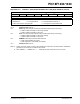
REGISTER 20-1: CONFIG1H: CONFIGURATION REGISTER 1 HIGH (BYTE ADDRESS 300001h)
R/P-0 R/P-0 U-0 U-0 R/P-0 R/P-1 R/P-1 R/P-1
IESO FCMEN
— — FOSC3 FOSC2 FOSC1 FOSC0
bit 7 bit 0
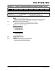
Legend:
R = Readable bit P = Programmable bit U = Unimplemented bit, read as ‘0’
-n = Value when device is unprogrammed u = Unchanged from programmed state
bit 7 IESO: Internal/External Oscillator Switchover bit
1 = Oscillator Switchover mode enabled
0 = Oscillator Switchover mode disabled
bit 6 FCMEN: Fail-Safe Clock Monitor Enable bit
1 = Fail-Safe Clock Monitor enabled
0 = Fail-Safe Clock Monitor disabled
bit 5-4 Unimplemented: Read as ‘0’
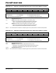
bit 3-0 FOSC3:FOSC0: Oscillator Selection bits
11xx = External RC oscillator, CLKO function on RA6
101x = External RC oscillator, CLKO function on RA6
1001 = Internal oscillator block, CLKO function on RA6, port function on RA7
1000 = Internal oscillator block, port function on RA6 and RA7
0111 = External RC oscillator, port function on RA6
0110 = HS oscillator, PLL enabled (Clock Frequency = 4 x FOSC1)
0101 = EC oscillator, port function on RA6
0100 = EC oscillator, CLKO function on RA6
0011 = External RC oscillator, CLKO function on RA6
0010 = HS oscillator
0001 = XT oscillator
0000 = LP oscillator