
Datasheet


PIC18F1230/1330
DS39758D-page 190 2009 Microchip Technology Inc.
19.5 Applications
In many applications, the ability to detect a drop below
a particular threshold is desirable.
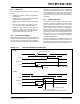
For general battery applications, Figure 19-3 shows a
possible voltage curve. Over time, the device voltage
decreases. When the device voltage reaches voltage
V
A, the LVD logic generates an interrupt at time TA. The
interrupt could cause the execution of an ISR, which
would allow the application to perform “housekeeping
tasks” and perform a controlled shutdown before the
device voltage exits the valid operating range at T
B.
The LVD, thus, would give the application a time win-
dow, represented by the difference between TA and TB,
to safely exit.
FIGURE 19-3: TYPICAL LOW-VOLTAGE
DETECT APPLICATION
19.6 Operation During Sleep
When enabled, the LVD circuitry continues to operate
during Sleep. If the device voltage crosses the trip
point, the LVDIF bit will be set and the device will wake-
up from Sleep. Device execution will continue from the
interrupt vector address if interrupts have been globally
enabled.
19.7 Effects of a Reset
A device Reset forces all registers to their Reset state.
This forces the LVD module to be turned off.
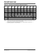
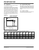
TABLE 19-1: REGISTERS ASSOCIATED WITH LOW-VOLTAGE DETECT MODULE
Time
Voltage
VA
VB
TA TB
VA = LVD trip point
VB = Minimum valid device
operating voltage
Legend:
Name Bit 7 Bit 6 Bit 5 Bit 4 Bit 3 Bit 2 Bit 1 Bit 0
Reset
Values
on Page:
LVDCON
— — IRVST LVDEN LVDL3 LVDL2 LVDL1 LVDL0 48
INTCON GIE/GIEH PEIE/GIEL TMR0IE INT0IE RBIE TMR0IF INT0IF RBIF 47
PIR2 OSCFIF — — EEIF —LVDIF— —49
PIE2
OSCFIE — — EEIE —LVDIE— —49
IPR2
OSCFIP — — EEIP —LVDIP— —49
Legend: — = unimplemented, read as ‘0’. Shaded cells are unused by the LVD module.