
Datasheet


PIC18F1230/1330
DS39758D-page 172 2009 Microchip Technology Inc.
The analog reference voltage is software selectable to
the device’s positive supply voltage (V
DD), or the
voltage level on the RA4/T0CKI/AN2/V
REF+ pin.
The A/D Converter has a unique feature of being able
to operate while the device is in Sleep mode. To
operate in Sleep, the A/D conversion clock must be
derived from the A/D Converter’s internal RC oscillator.
The output of the sample and hold is the input into the
A/D Converter, which generates the result via succes-
sive approximation.
A device Reset forces all registers to their Reset state.
This forces the A/D module to be turned off and any
conversion in progress is aborted.
Each port pin associated with the A/D Converter can be
configured as an analog input or as a digital I/O. The
ADRESH and ADRESL registers contain the result of
the A/D conversion. When the A/D conversion is
complete, the result is loaded into the
ADRESH:ADRESL register pair, the GO/DONE
bit
(ADCON0 register) is cleared and A/D Interrupt Flag bit,
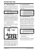
ADIF, is set. The block diagram of the A/D module is
shown in Figure 16-1.
FIGURE 16-1: A/D BLOCK DIAGRAM
(Input Voltage)
VAIN
VREF+
Reference
Voltage
AV
DD
VCFG0
CHS1:CHS0
AN3
AN2
AN1
AN0
0011
0010
0001
0000
10-Bit
A/D
AVSS
Converter
1
0