
Datasheet


PIC18F1230/1330
DS39758D-page 136 2009 Microchip Technology Inc.
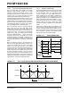
14.7.2 DEAD-TIME RANGES
The amount of dead time provided by the dead-time
unit is selected by specifying the input clock prescaler
value and a 6-bit unsigned value defined in the DTCON
register. Four input clock prescaler selections have
been provided to allow a suitable range of dead times
based on the device operating frequency. F
OSC/2,
F
OSC/4, FOSC/8 and FOSC/16 are the clock prescaler
options available using the DTPS1:DTPS0 control bits
in the DTCON register.
After selecting an appropriate prescaler value, the
dead time is adjusted by loading a 6-bit unsigned value
into DTCON<5:0>. The dead-time unit prescaler is
cleared on any of the following events:
• On a load of the down timer due to a duty cycle
comparison edge event;
• On a write to the DTCON register; or
• On any device Reset.
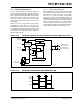
14.7.3 DECREMENTING THE DEAD-TIME
COUNTER
The dead-time counter is clocked from any of the
Q clocks based on the following conditions.
1. The dead-time counter is clocked on Q1 when:
• The DTPS bits are set to any of the following
dead-time prescaler settings: F
OSC/4,
F
OSC/8, FOSC/16
• The PWM Time Base Prescale bits
(PTCKPS<1:0>) are set to any of the following
prescale ratios: F
OSC/16, FOSC/64, FOSC/256
2. The dead-time counter is clocked by a pair of
Q clocks when the PWM Time Base Prescale
bits are set to 1:1 (PTCKPS<1:0> = 00, F
OSC/4)
and the dead-time counter is clocked by the
FOSC/2 (DTPS<1:0> = 00).
3. The dead-time counter is clocked using every
other Q clock, depending on the two LSbs in the
Duty Cycle registers:
• If the PWM duty cycle match occurs on Q1 or
Q3, then the dead-time counter is clocked
using every Q1 and Q3
• If the PWM duty cycles match occurs on Q2
or Q4, then the dead-time counter is clocked
using every Q2 and Q4
4. When the DTPS<1:0> bits are set to any of the
other dead-time prescaler settings (i.e., F
OSC/4,
F
OSC/8 or FOSC/16) and the PWM time base pres-
caler is set to 1:1, the dead-time counter is clocked
by the Q clock corresponding to the Q clocks on
which the PWM duty cycle match occurs.
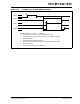
REGISTER 14-5: DTCON: DEAD-TIME CONTROL REGISTER
R/W-0 R/W-0 R/W-0 R/W-0 R/W-0 R/W-0 R/W-0 R/W-0
DTPS1 DTPS0 DT5 DT4 DT3 DT2 DT1 DT0
bit 7 bit 0
Legend:
R = Readable bit W = Writable bit U = Unimplemented bit, read as ‘0’
-n = Value at POR ‘1’ = Bit is set ‘0’ = Bit is cleared x = Bit is unknown
bit 7-6 DTPS1:DTPS0: Dead-Time Unit A Prescale Select bits
11 = Clock source for dead-time unit is F
OSC/16
10 = Clock source for dead-time unit is F
OSC/8
01 = Clock source for dead-time unit is F
OSC/4
00 = Clock source for dead-time unit is F
OSC/2
bit 5-0 DT5:DT0: Unsigned 6-Bit Dead-Time Value for Dead-Time Unit bits