
Datasheet


PIC18F1230/1330
2009 Microchip Technology Inc. DS39758D-page 13
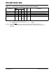
TABLE 1-2: PIC18F1230/1330 PINOUT I/O DESCRIPTIONS
Pin Name
Pin Number
Pin
Type
Buffer
Type
Description
PDIP,
SOIC
SSOP QFN
MCLR
/VPP/RA5/FLTA
MCLR
VPP
RA5
FLTA
(1)
441
I
I
I
I
ST
Analog
ST
ST
Master Clear (input), programming voltage (input)
or Fault detect input.
Master Clear (Reset) input. This pin is an
active-low Reset to the device.
Programming voltage input.
Digital input.
Fault detect input for PWM.
RA7/OSC1/CLKI/
T1OSI/FLTA
RA7
OSC1
CLKI
T1OSI
(2)
FLTA
(1)
16 18 21
I/O
I
I
I
I
ST
Analog
—
Analog
ST
Oscillator crystal, external clock input, Timer1
oscillator input or Fault detect input.
Digital I/O.
Oscillator crystal input or external clock source
input.
External clock source input.
Timer1 oscillator input.
Fault detect input for PWM.
RA6/OSC2/CLKO/
T1OSO/T1CKI/AN3
RA6
OSC2
CLKO
T1OSO
(2)
TICKI
(2)
AN3
15 17 20
I/O
O
O
O
I
I
ST
—
—
—
ST
Analog
Oscillator crystal, clock output, Timer1 oscillator
output or analog input.
Digital I/O.
Oscillator crystal output or external clock
source input.
External clock source output.
Timer1 oscillator output.
Timer1 clock input.
Analog input 3.
Legend: TTL = TTL compatible input CMOS = CMOS compatible input or output
ST = Schmitt Trigger input with CMOS levels I = Input
O = Output P = Power
Note 1: Placement of FLTA
depends on the value of Configuration bit, FLTAMX, of CONFIG3H.
2: Placement of T1OSI and T1OSO/T1CKI depends on the value of Configuration bit, T1OSCMX, of
CONFIG3H.