
Datasheet


PIC18F1230/1330
2009 Microchip Technology Inc. DS39758D-page 107
12.0 TIMER0 MODULE
The Timer0 module has the following features:
• Software selectable as an 8-bit or
16-bit timer/counter
• Readable and writable
• Dedicated 8-bit software programmable prescaler
• Clock source selectable to be external or internal
• Interrupt on overflow from FFh to 00h in 8-bit
mode and FFFFh to 0000h in 16-bit mode
• Edge select for external clock
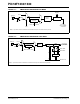
Figure 12-1 shows a simplified block diagram of the
Timer0 module in 8-bit mode and Figure 12-2 shows a
simplified block diagram of the Timer0 module in 16-bit
mode.
The T0CON register (Register 12-1) is a readable and
writable register that controls all the aspects of Timer0,
including the prescale selection.
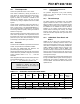
REGISTER 12-1: T0CON: TIMER0 CONTROL REGISTER
R/W-1 R/W-1 R/W-1 R/W-1 R/W-1 R/W-1 R/W-1 R/W-1
TMR0ON T016BIT T0CS T0SE PSA T0PS2 T0PS1 T0PS0
bit 7 bit 0
Legend:
R = Readable bit W = Writable bit U = Unimplemented bit, read as ‘0’
-n = Value at POR ‘1’ = Bit is set ‘0’ = Bit is cleared x = Bit is unknown
bit 7 TMR0ON: Timer0 On/Off Control bit
1 = Enables Timer0
0 = Stops Timer0
bit 6 T016BIT: Timer0 16-Bit Control bit
1 = Timer0 is configured as an 8-bit timer/counter
0 = Timer0 is configured as a 16-bit timer/counter
bit 5 T0CS: Timer0 Clock Source Select bit
1 = Transition on T0CKI pin input edge
0 = Internal clock (F
OSC/4)
bit 4 T0SE: Timer0 Source Edge Select bit
1 = Increment on high-to-low transition on T0CKI pin
0 = Increment on low-to-high transition on T0CKI pin
bit 3 PSA: Timer0 Prescaler Assignment bit
1 = TImer0 prescaler is NOT assigned. Timer0 clock input bypasses prescaler.
0 = Timer0 prescaler is assigned. Timer0 clock input comes from prescaler output.
bit 2-0 T0PS2:T0PS0: Timer0 Prescaler Select bits
111 = 1:256 Prescale value
110 = 1:128 Prescale value
101 = 1:64 Prescale value
100 = 1:32 Prescale value
011 = 1:16 Prescale value
010 = 1:8 Prescale value
001 = 1:4 Prescale value
000 = 1:2 Prescale value