
Information
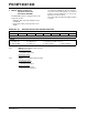
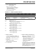


© 2008 Microchip Technology Inc. DS80352B-page 3
PIC18F1230/1330
4. Module: 10-Bit Analog-to-Digital
Converter (A/D)
Register 15-2 is modified as shown to:
• Change the bit designations of ADCON<2:0>
(PCFG2, PCFG1 and PCFG0) to R/W-0, to
match PCFG3 (ADCON<3>)
• Remove the notes for ADCON<3:0>
The new text appears in bold.
5. Module: Comparator
In Section 16.6 “Comparator Interrupts”, the
procedure for clearing the interrupt in the Interrupt
Service Routine is modified with the new text
shown in bold.
a) End the mismatch condition by doing either of
the following:
- Reading or writing to CMCON
- Returning the input to its original state
b) Clear flag bit CMPxIF
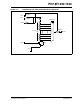
6. Module: Comparator Voltage Reference
Section 17.1 “Configuring the Comparator
Voltage Reference” is changed to:
• Add new text and a table (Table 17-1) about the
voltage reference being able to select the
unscaled V
REF+ for comparator input
• Modify Register 17-1 (CVRCON) with a new
description of bit 4 (CVRSS)
• Revise Figure 17-1
The textual changes break the last sentence of the
first paragraph of Section 17.1 “Configuring the
Comparator Voltage Reference” into a second
paragraph and adds content. The incorporation of
the three bulleted changes are shown, with new or
altered text indicated by bold face.
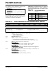
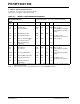
REGISTER 15-2: ADCON1: A/D CONTROL REGISTER 1
U-0 U-0 U-0 R/W-0 R/W-0 R/W-0 R/W-0 R/W-0
— — — VCFG0 PCFG3 PCFG2 PCFG1 PCFG0
bit 7 bit 0
Legend:
R = Readable bit W = Writable bit U = Unimplemented bit, read as ‘0’
-n = Value at POR ‘1’ = Bit is set ‘0’ = Bit is cleared x = Bit is unknown
bit 7-5 Unimplemented: Read as ‘0’
bit 4 VCFG0: Voltage Reference Configuration bit (VREF+ source)
1 = Positive reference for the A/D is V
REF+
0 = Positive reference for the A/D is AV
DD
bit 3 PCFG3: A/D Port Configuration bit for RA6/AN3
0 = Port is configured as AN3
1 = Port is configured as RA6
bit 2 PCFG2: A/D Port Configuration bit for RA4/AN2
0 = Port is configured as AN2
1 = Port is configured as RA4
bit 1 PCFG1: A/D Port Configuration bit for RA1/AN1
0 = Port is configured as AN1
1 = Port is configured as RA1
bit 0 PCFG0: A/D Port Configuration bit for RA0/AN0
0 = Port is configured as AN0
1 = Port is configured as RA0