
Information


© 2008 Microchip Technology Inc. DS80352B-page 1
PIC18F1230/1330
Clarifications/Corrections to the Data
Sheet:
In the Device Data Sheet (DS39758C), the following
clarifications and corrections should be noted. Any
silicon issues related to the PIC18F1230/1330 will be
reported in a separate silicon errata. Please check the
Microchip web site for any existing issues.
1. Module: Oscillator Configurations – PLL
The second paragraph of Section 2.6.4 “PLL in
INTOSC Modes”, is modified by the addition of
new text shown in bold.
Unlike HSPLL mode, the PLL is controlled through
software. The control bit, PLLEN (OSCTUNE<6>), is
used to enable or disable its operation. If PLL is
enabled and a Two-Speed Start-up from wake is
performed, execution is delayed until the PLL
starts.
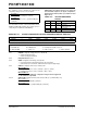
2. Module: Flash Program Memory
In Section 6.2.4 “Table Pointer Boundaries”,
the third paragraph and Figure 6-3 are modified:
• The paragraph is modified by the removal of the
first sentence and the addition of new text
shown in bold.
When the timed write to program memory begins (via
the WR bit), the 19 MSbs of the TBLPTR
(TBLPTR<21:3>) determine which program memory
block of 8 bytes is written to. The Table Pointer
register’s three LSBs (TBLPTR<2:0>) are ignored.
For more detail, see Section 6.5 “Writing to Flash
Program Memory”.
• Figure 6-3 is modified as shown.
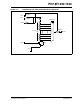
FIGURE 6-3: TABLE POINTER BOUNDARIES BASED ON OPERATION
21 16 15 87 0
TABLE ERASE
TABLE WRITE
TABLE READ – TBLPTR<21:0>
TBLPTRL
TBLPTRH
TBLPTRU
TBLPTR<21:3>
TBLPTR<21:6>
PIC18F1230/1330 Data Sheet Errata