
Information


Table Of Contents
PIC16F87/88
DS80171L-page 4 © 2008 Microchip Technology Inc.
6. Module: PORTB, RB6 Pin
During normal operating conditions, extra current
will be consumed on the PIC16F87/88 device’s
power source (VDD) when the PORTB, RB6 pin is
configured as an analog input (AN5) and is
connected to an analog source. A/D operation on
RB6 or any of the other analog I/O pins will not be
affected by this extra current. The extra current is
due to the T1CKI Schmitt Trigger not being
disabled when RB6 is configured as an analog pin.
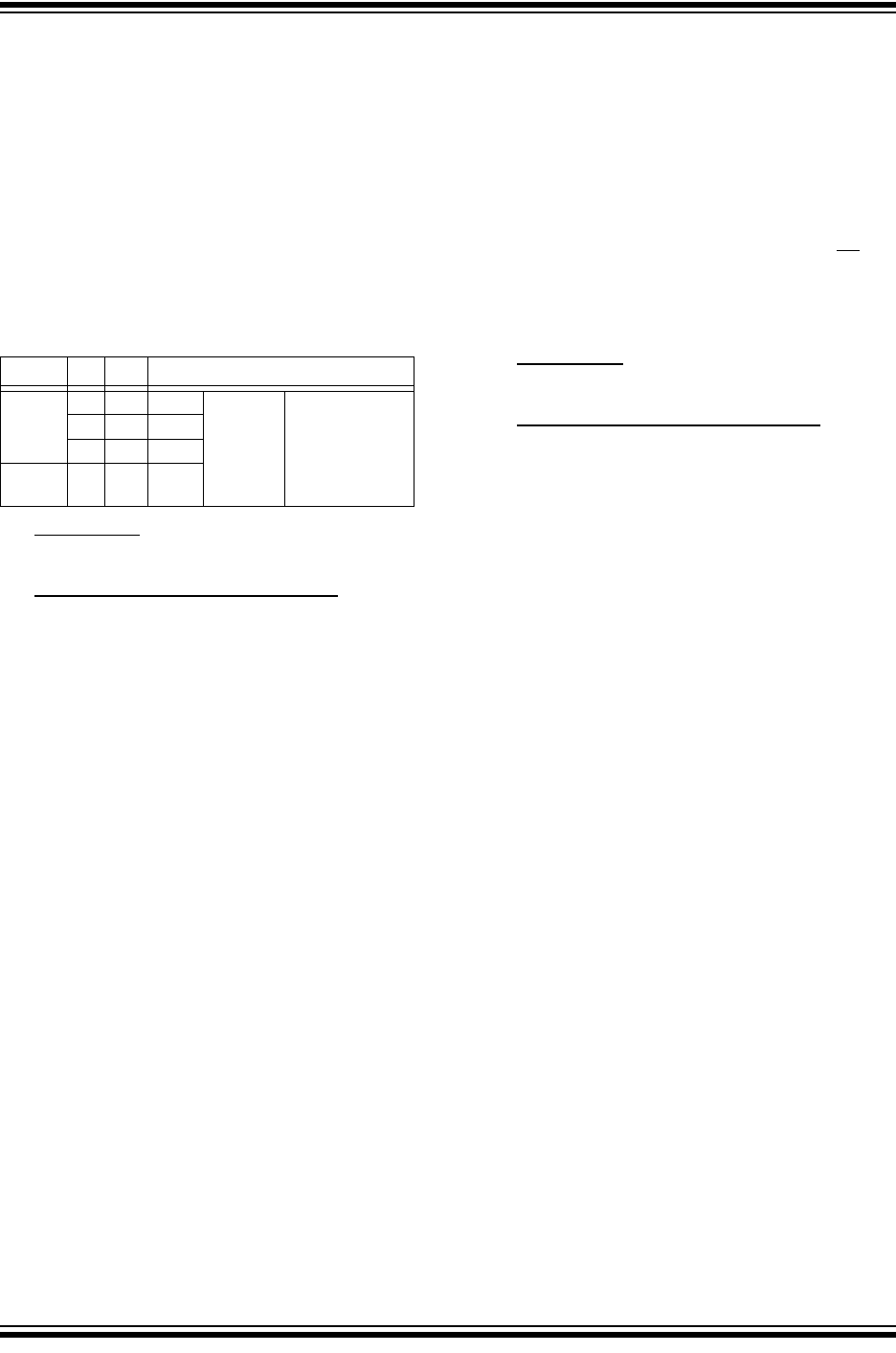
The amount of additional current observed will be
dependent on the analog voltage present on the
AN5 pin. The following table illustrates this
additional current across operating temperatures:
Work around
None
Date Codes that pertain to this issue:
All date codes associated with silicon revision B1.
This issue is not found in devices with silicon
revision C2 (Revision ID 0 1000) or later.
7. Module: PORTB Interrupts
When the PORTB interrupt-on-change feature and
a PORTB peripheral are enabled simultaneously,
the PORTB peripheral input signal’s rising and
falling edges will trigger an interrupt-on-change
event. This is due to the interrupt-on-change
feature not being disabled on the respective pin for
that peripheral when it is enabled.
The affected pins and peripheral signals on
PORTB are RB4: SCK and SCL, RB5: SS
and
RB6: T1CKI. The functionality of T1OSI (RB7),
T1OSO (RB6) and TX/CK (RB5) is not affected by
this issue.
Work around
None
Date Codes that pertain to this issue:
All date codes associated with silicon revision B1.
This issue is not found in devices with silicon
revision C2 (Revision ID 0 1000) or later.
Max Units Conditions
All
Devices
1.4 mA -40°C
V
DD
= 5.5V AN5 = 0.6-0.7 V
DD
1.3 mA +25°C
1.1 mA +85°C
Extended
Devices
0.9 mA +125°C