
Datasheet


© 2007 Microchip Technology Inc. DS41250F-page 143
PIC16F913/914/916/917/946
10.0 LIQUID CRYSTAL DISPLAY
(LCD) DRIVER MODULE
The Liquid Crystal Display (LCD) driver module
generates the timing control to drive a static or
multiplexed LCD panel. In the PIC16F913/916 devices,
the module drives the panels of up to four commons
and up to 16 segments. In the PIC16F914/917 devices,
the module drives the panels of up to four commons
and up to 24 segments. In the PIC16F946 device, the
module drives the panels of up to four commons and up
to 42 segments. The LCD module also provides control
of the LCD pixel data.
The LCD driver module supports:
• Direct driving of LCD panel
• Three LCD clock sources with selectable prescaler
• Up to four commons:
- Static (1 common)
- 1/2 multiplex (2 commons)
- 1/3 multiplex (3 commons)
- 1/4 multiplex (4 commons)
• Segments up to:
- 16 (PIC16F913/916)
- 24 (PIC16F914/917)
- 42 (PIC16F946)
• Static, 1/2 or 1/3 LCD Bias
10.1 LCD Registers
The module contains the following registers:
• LCD Control Register (LCDCON)
• LCD Phase Register (LCDPS)
• Up to 6 LCD Segment Enable Registers (LCDSEn)
• Up to 24 LCD Data Registers (LCDDATA)
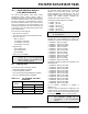
TABLE 10-1: LCD SEGMENT AND DATA
REGISTERS
The LCDCON register (Register 10-1) controls the
operation of the LCD driver module. The LCDPS
register (Register 10-2) configures the LCD clock
source prescaler and the type of waveform; Type-A or
Type-B. The LCDSE registers (Register 10-3)
configure the functions of the port pins.
The following LCDSE registers are available:
• LCDSE0 SE<7:0>
• LCDSE1 SE<15:8>
• LCDSE2 SE<23:16>
(1)
• LCDSE3 SE<31:24>
(2)
• LCDSE4 SE<39:32>
(2)
• LCDSE5 SE<41:40>
(2)
Once the module is initialized for the LCD panel, the
individual bits of the LCDDATA<11:0> registers are
cleared/set to represent a clear/dark pixel, respectively:
• LCDDATA0 SEG<7:0>COM0
• LCDDATA1 SEG<15:8>COM0
• LCDDATA2 SEG<23:16>COM0
• LCDDATA3 SEG<7:0>COM1
• LCDDATA4 SEG<15:8>COM1
• LCDDATA5 SEG<23:16>COM1
• LCDDATA6 SEG<7:0>COM2
• LCDDATA7 SEG<15:8>COM2
• LCDDATA8 SEG<23:16>COM2
• LCDDATA9 SEG<7:0>COM3
• LCDDATA10 SEG<15:8>COM3
• LCDDATA11 SEG<23:16>COM3
The following additional registers are available on the
PIC16F946 only:
• LCDDATA12 SEG<31:24>COM0
• LCDDATA13 SEG<39:32>COM0
• LCDDATA14 SEG<41:40>COM0
• LCDDATA15 SEG<31:24>COM1
• LCDDATA16 SEG<39:32>COM1
• LCDDATA17 SEG<41:40>COM1
• LCDDATA18 SEG<31:24>COM2
• LCDDATA19 SEG<39:32>COM2
• LCDDATA20 SEG<41:40>COM2
• LCDDATA21 SEG<31:24>COM3
• LCDDATA22 SEG<39:32>COM3
• LCDDATA23 SEG<41:40>COM3
As an example, LCDDATAx is detailed in
Register 10-4.
Once the module is configured, the LCDEN bit of the
LCDCON register is used to enable or disable the LCD
module. The LCD panel can also operate during Sleep
by clearing the SLPEN
bit of the LCDCON register.
Note: COM3 and SEG15 share the same
physical pin on the PIC16F913/916,
therefore SEG15 is not available when
using 1/4 multiplex displays.
Device
# of LCD Registers
Segment Enable
Data
PIC16F913/916 2 8
PIC16F914/917 3 12
PIC16F946 6 24
Note 1: PIC16F914/917 and PIC16F946 only.
2: PIC16F946 only.
Note: The LCDDATA2, LCDDATA5, LCDDATA8
and LCDDATA11 registers are not
implemented in the PIC16F913/916
devices.