
Datasheet


© 2007 Microchip Technology Inc. DS41250F-page 139
PIC16F913/914/916/917/946
9.3.2 SYNCHRONOUS SLAVE MODE
The following bits are used to configure the AUSART
for Synchronous slave operation:
• SYNC = 1
• CSRC = 0
• SREN = 0 (for transmit); SREN = 1 (for receive)
• CREN = 0 (for transmit); CREN = 1 (for receive)
• SPEN = 1
Setting the SYNC bit of the TXSTA register configures the
device for synchronous operation. Clearing the CSRC bit
of the TXSTA register configures the device as a slave.
Clearing the SREN and CREN bits of the RCSTA register
ensures that the device is in the Transmit mode,
otherwise the device will be configured to receive. Setting
the SPEN bit of the RCSTA register enables the
AUSART.
The LCD SEG8 and SEG9 functions must be disabled
by clearing the SE8 and SE9 bits of the LCDSE1
register, if the RX/DT and TX/CK pins are shared with
the LCD peripheral.
9.3.2.1 AUSART Synchronous Slave
Transmit
The operation of the Synchronous Master and Slave
modes are identical (see Section 9.3.1.2 “Synchronous
Master Transmission”), except in the case of the Sleep
mode.
If two words are written to the TXREG and then the
SLEEP instruction is executed, the following will occur:
1. The first character will immediately transfer to
the TSR register and transmit.
2. The second word will remain in TXREG register.
3. The TXIF bit will not be set.
4. After the first character has been shifted out of
TSR, the TXREG register will transfer the second
character to the TSR and the TXIF bit will now be
set.
5. If the PEIE and TXIE bits are set, the interrupt
will wake the device from Sleep and execute the
next instruction. If the GIE bit is also set, the
program will call the Interrupt Service Routine.
9.3.2.2 Synchronous Slave Transmission
Set-up:
1. Set the SYNC and SPEN bits and clear the
CSRC bit.
2. Clear the CREN and SREN bits.
3. If using interrupts, ensure that the GIE and PEIE
bits of the INTCON register are set and set the
TXIE bit.
4. If 9-bit transmission is desired, set the TX9 bit.
5. Enable transmission by setting the TXEN bit.
6. Verify address detection is disabled by clearing
the ADDEN bit of the RCSTA register.
7. If 9-bit transmission is selected, insert the Most
Significant bit into the TX9D bit.
8. Start transmission by writing the Least
Significant 8 bits to the TXREG register.
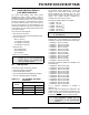
TABLE 9-8: REGISTERS ASSOCIATED WITH SYNCHRONOUS SLAVE TRANSMISSION
NameBit 7Bit 6Bit 5Bit 4Bit 3Bit 2Bit 1Bit 0
Value on
POR, BOR
Value on
all other
Resets
INTCON GIE PEIE
T0IE INTE RBIE T0IF INTF RBIF 0000 000x 0000 000x
LCDCON LCDEN
SLPEN WERR VLCDEN CS1 CS0 LMUX1 LMUX0 0001 0011 0001 0011
LCDSE1
SE15 SE14 SE13 SE12 SE11 SE10 SE9 SE8 0000 0000 0000 0000
PIE1
EEIE ADIE RCIE TXIE SSPIE CCP1IE TMR2IE TMR1IE 0000 0000 0000 0000
PIR1
EEIF ADIF RCIF TXIF SSPIF CCP1IF TMR2IF TMR1IF 0000 0000 0000 0000
RCSTA SPEN
RX9 SREN CREN ADDEN FERR OERR RX9D 0000 000X 0000 000X
SSPCON
WCOL SSPOV SSPEN CKP SSPM3 SSPM2 SSPM1 SSPM0 0000 0000 0000 0000
TRISC TRISC7 TRISC6
TRISC5 TRISC4 TRISC3 TRISC2 TRISC1 TRISC0 1111 1111 1111 1111
TXREG AUSART Transmit Data Register 0000 0000 0000 0000
TXSTA CSRC TX9 TXEN SYNC
— BRGH TRMT TX9D 0000 -010 0000 -010
Legend: x = unknown, - = unimplemented read as ‘0’. Shaded cells are not used for Synchronous Slave Transmission.