
Datasheet


PIC16F913/914/916/917/946
DS41250F-page 102 © 2007 Microchip Technology Inc.
6.0 TIMER1 MODULE WITH GATE
CONTROL
The Timer1 module is a 16-bit timer/counter with the
following features:
• 16-bit timer/counter register pair (TMR1H:TMR1L)
• Programmable internal or external clock source
• 3-bit prescaler
• Optional LP oscillator
• Synchronous or asynchronous operation
• Timer1 gate (count enable) via comparator or
T1G
pin
• Interrupt on overflow
• Wake-up on overflow (external clock,
Asynchronous mode only)
• Clock source for LCD module
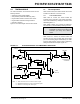
Figure 6-1 is a block diagram of the Timer1 module.
6.1 Timer1 Operation
The Timer1 module is a 16-bit incrementing counter
which is accessed through the TMR1H:TMR1L register
pair. Writes to TMR1H or TMR1L directly update the
counter.
When used with an internal clock source, the module is
a timer. When used with an external clock source, the
module can be used as either a timer or counter.
6.2 Clock Source Selection
The TMR1CS bit of the T1CON register is used to select
the clock source. When TMR1CS = 0, the clock source
is F
OSC/4. When TMR1CS = 1, the clock source is
supplied externally.
FIGURE 6-1: TIMER1 BLOCK DIAGRAM
Clock Source TMR1CS
F
OSC/4 0
T1CKI pin 1
TMR1H TMR1L
T1SYNC
T1CKPS<1:0>
Prescaler
1, 2, 4, 8
0
1
Synchronized
clock input
2
Set flag bit
TMR1IF on
Overflow
TMR1
(2)
TMR1GE
TMR1ON
1
0
SYNCC2OUT
(4)
T1GSS
T1GINV
To C2 Comparator Module
Timer1 Clock
Note 1: ST Buffer is low power type when using LP oscillator, or high speed type when using T1CKI.
2: Timer1 register increments on rising edge.
3: Synchronize does not operate while in Sleep.
4: SYNCC2OUT is synchronized when the C2SYNC bit of the CMCON1 register is set.
EN
T1G
LP OSC
F
OSC/4
Internal
Clock
1
0
OSC1/T1OSI
OSC2/T1OSO
FOSC = 000
T1OSCEN
FOSC = x00
1
0
T1CKI
TMR1CS
(1)
To LCD Module
Synchronize
(3)
det