
Datasheet


Table Of Contents
- High-Performance RISC CPU:
- Special Microcontroller Features:
- Low-Power Features:
- Peripheral Features:
- Pin Diagrams – PIC16F882/883/886, 28-Pin PDIP, SOIC, SSOP
- Pin Diagrams – PIC16F882/883/886, 28-Pin QFN
- Pin Diagrams – PIC16F884/887, 40-Pin PDIP
- Pin Diagrams – PIC16F884/887, 44-Pin QFN
- Pin Diagrams – PIC16F884/887, 44-Pin TQFP
- Most Current Data Sheet
- Errata
- Customer Notification System
- 1.0 Device Overview
- 2.0 Memory Organization
- 2.1 Program Memory Organization
- 2.2 Data Memory Organization
- 2.2.1 General Purpose Register File
- 2.2.2 Special Function Registers
- FIGURE 2-4: PIC16F882 Special Function Registers
- FIGURE 2-5: PIC16F883/PIC16F884 Special Function Registers
- FIGURE 2-6: PIC16F886/PIC16F887 Special Function Registers
- TABLE 2-1: PIC16F882/883/884/886/887 Special Function Registers Summary Bank 0
- TABLE 2-2: PIC16F882/883/884/886/887 Special Function Registers Summary Bank 1
- TABLE 2-3: PIC16F882/883/884/886/887 Special Function Registers Summary Bank 2
- TABLE 2-4: PIC16F882/883/884/886/887 Special Function Registers Summary Bank 3
- Register 2-1: STATUS: STATUS Register
- Register 2-2: OPTION_REG: OPTION Register
- Register 2-3: INTCON: Interrupt Control Register
- Register 2-4: PIE1: Peripheral Interrupt Enable Register 1
- Register 2-5: PIE2: Peripheral Interrupt Enable Register 2
- Register 2-6: PIR1: Peripheral Interrupt Request Register 1
- Register 2-7: PIR2: Peripheral Interrupt Request Register 2
- Register 2-8: PCON: Power Control Register
- 2.3 PCL and PCLATH
- 2.4 Indirect Addressing, INDF and FSR Registers
- 3.0 I/O Ports
- 3.1 PORTA and the TRISA Registers
- 3.2 Additional Pin Functions
- 3.2.1 ANSEL Register
- 3.2.2 Ultra Low-Power Wake-up
- 3.2.3 Pin Descriptions and Diagrams
- FIGURE 3-1: Block Diagram of RA0
- FIGURE 3-2: Block Diagram of RA1
- FIGURE 3-3: Block Diagram of RA2
- FIGURE 3-4: Block Diagram of RA3
- FIGURE 3-5: Block Diagram of RA4
- FIGURE 3-6: Block Diagram of RA5
- FIGURE 3-7: Block Diagram of RA6
- FIGURE 3-8: Block Diagram of RA7
- TABLE 3-1: Summary of Registers Associated with PORTA
- 3.3 PORTB and TRISB Registers
- 3.4 Additional PORTB Pin Functions
- 3.5 PORTC and TRISC Registers
- 3.6 PORTD and TRISD Registers
- 3.7 PORTE and TRISE Registers
- 4.0 Oscillator Module (With Fail-Safe Clock Monitor)
- 5.0 Timer0 Module
- 6.0 Timer1 Module with Gate Control
- 6.1 Timer1 Operation
- 6.2 Clock Source Selection
- 6.3 Timer1 Prescaler
- 6.4 Timer1 Oscillator
- 6.5 Timer1 Operation in Asynchronous Counter Mode
- 6.6 Timer1 Gate
- 6.7 Timer1 Interrupt
- 6.8 Timer1 Operation During Sleep
- 6.9 ECCP Capture/Compare Time Base
- 6.10 ECCP Special Event Trigger
- 6.11 Comparator Synchronization
- 6.12 Timer1 Control Register
- 7.0 Timer2 Module
- 8.0 Comparator Module
- 8.1 Comparator Overview
- 8.2 Comparator Control
- 8.3 Comparator Response Time
- 8.4 Comparator Interrupt Operation
- 8.5 Operation During Sleep
- 8.6 Effects of a Reset
- 8.7 Analog Input Connection Considerations
- 8.8 Additional Comparator Features
- 8.9 Comparator SR Latch
- 8.10 Comparator Voltage Reference
- 8.10.1 Independent Operation
- 8.10.2 Output Voltage Selection
- 8.10.3 Output Clamped to Vss
- 8.10.4 Output Ratiometric to Vdd
- 8.10.5 Fixed Voltage Reference
- 8.10.6 Fixed Voltage Reference Stabilization Period
- 8.10.7 Voltage Reference Selection
- FIGURE 8-8: Comparator Voltage Reference Block Diagram
- FIGURE 8-9: Comparator and ADC Voltage REference Block Diagram
- TABLE 8-2: Comparator and ADC Voltage Reference Priority
- Register 8-5: VRCON: Voltage Reference Control register
- TABLE 8-3: Summary of Registers Associated with the Comparator and Voltage Reference Modules
- 9.0 Analog-to-Digital Converter (ADC) Module
- FIGURE 9-1: ADC Block Diagram
- 9.1 ADC Configuration
- 9.2 ADC Operation
- 9.2.1 Starting a Conversion
- 9.2.2 Completion of a Conversion
- 9.2.3 Terminating a conversion
- 9.2.4 ADC Operation During Sleep
- 9.2.5 Special Event Trigger
- 9.2.6 A/D Conversion Procedure
- 9.2.7 ADC Register Definitions
- Register 9-1: ADCON0: A/D Control Register 0
- Register 9-2: ADCON1: A/D Control Register 1
- Register 9-3: ADRESH: ADC Result Register High (ADRESH) ADFM = 0
- Register 9-4: ADRESL: ADC Result Register Low (ADRESL) ADFM = 0
- Register 9-5: ADRESH: ADC Result Register High (ADRESH) ADFM = 1
- Register 9-6: ADRESL: ADC Result Register Low (ADRESL) ADFM = 1
- 9.3 A/D Acquisition Requirements
- 10.0 Data EEPROM and Flash Program Memory Control
- 10.1 EEADR and EEADRH Registers
- 10.2 Writing to Flash Program Memory
- 10.3 Write Verify
- 10.4 Protection Against Spurious Write
- 10.5 Data EEPROM Operation During Code-Protect
- 11.0 Capture/Compare/PWM Modules (CCP1 and CCP2)
- 11.1 Enhanced Capture/Compare/PWM (CCP1)
- 11.2 Capture/Compare/PWM (CCP2)
- 11.3 Capture Mode
- 11.4 Compare Mode
- 11.5 PWM Mode
- 11.6 PWM (Enhanced Mode)
- FIGURE 11-5: Example Simplified Block Diagram of the Enhanced PWM Mode
- TABLE 11-5: Example Pin Assignments for Various PWM Enhanced Modes
- FIGURE 11-6: Example PWM (enhanced Mode) Output Relationships (Active-High State)
- FIGURE 11-7: Example Enhanced PWM Output Relationships (Active-Low State)
- 11.6.1 Half-Bridge Mode
- 11.6.2 Full-Bridge Mode
- 11.6.3 Start-up Considerations
- 11.6.4 Enhanced PWM Auto- shutdown mode
- 11.6.5 Auto-Restart Mode
- 11.6.6 Programmable Dead-Band Delay Mode
- 11.6.7 Pulse Steering Mode
- Register 11-5: PSTRCON: Pulse Steering Control Register(1)
- FIGURE 11-19: Simplified Steering Block Diagram
- FIGURE 11-20: Example of Steering Event at End of Instruction (STRSYNC = 0)
- FIGURE 11-21: Example of Steering Event at Beginning of Instruction (STRSYNC = 1)
- TABLE 11-6: Registers Associated with Capture, cOMPARE and Timer1
- TABLE 11-7: Registers Associated with PWM and Timer2
- 12.0 Enhanced Universal Synchronous Asynchronous Receiver Transmitter (EUSART)
- FIGURE 12-1: EUSART Transmit Block Diagram
- FIGURE 12-2: EUSART Receive Block Diagram
- 12.1 EUSART Asynchronous Mode
- 12.2 Clock Accuracy with Asynchronous Operation
- 12.3 EUSART Baud Rate Generator (BRG)
- 12.4 EUSART Synchronous Mode
- 12.5 EUSART Operation During Sleep
- 13.0 Master Synchronous Serial Port (MSSP) Module
- 13.1 Master SSP (MSSP) Module Overview
- 13.2 Control Registers
- 13.3 SPI Mode
- 13.4 MSSP I2C Operation
- FIGURE 13-6: MSSP Block Diagram (I2C Mode)
- 13.4.1 SLAVE Mode
- 13.4.2 General Call Address Support
- 13.4.3 Master Mode
- 13.4.4 I2C™ Master Mode Support
- 13.4.5 Baud Rate Generator
- 13.4.6 I2C™ Master Mode Start Condition Timing
- 13.4.7 I2C™ Master Mode Repeated Start Condition Timing
- 13.4.8 I2C™ Master Mode Transmission
- 13.4.9 I2C™ Master Mode Reception
- 13.4.10 Acknowledge Sequence Timing
- 13.4.11 Stop Condition Timing
- 13.4.12 Clock Arbitration
- 13.4.13 Sleep Operation
- 13.4.14 Effect of a Reset
- 13.4.15 Multi-Master Mode
- 13.4.16 Multi -Master Communication, Bus Collision, and Bus Arbitration
- FIGURE 13-20: Bus Collision Timing for Transmit and Acknowledge
- FIGURE 13-21: Bus Collision During Start Condition (SDA only)
- FIGURE 13-22: Bus Collision During Start Condition (SCL = 0)
- FIGURE 13-23: BRG Reset Due to SDA Arbitration During Start Condition
- FIGURE 13-24: Bus Collision During a Repeated Start Condition (Case 1)
- FIGURE 13-25: Bus Collision During Repeated Start Condition (Case 2)
- FIGURE 13-26: Bus Collision During a Stop Condition (Case 1)
- FIGURE 13-27: Bus Collision During a Stop Condition (Case 2)
- 13.4.17 SSP Mask Register
- 14.0 Special Features of the CPU
- 14.1 Configuration Bits
- 14.2 Reset
- FIGURE 14-1: Simplified Block Diagram of On-chip Reset Circuit
- 14.2.1 Power-on Reset (POR)
- 14.2.2 MCLR
- 14.2.3 Power-up Timer (PWRT)
- 14.2.4 Brown-out Reset (BOR)
- 14.2.5 Time-out Sequence
- 14.2.6 Power Control (PCON) Register
- TABLE 14-1: Time-out in Various Situations
- TABLE 14-2: Status/PCON Bits and Their Significance
- TABLE 14-3: Summary of Registers Associated with Brown-out
- FIGURE 14-4: Time-out Sequence On Power-up (Delayed MCLR): Case 1
- FIGURE 14-5: Time-out Sequence On Power-up (Delayed MCLR): Case 2
- FIGURE 14-6: Time-out Sequence on Power-up (MCLR with Vdd)
- TABLE 14-4: Initialization Condition for Register
- TABLE 14-5: Initialization Condition for Special Registers
- 14.3 Interrupts
- 14.4 Context Saving During Interrupts
- 14.5 Watchdog Timer (WDT)
- 14.6 Power-Down Mode (Sleep)
- 14.7 Code Protection
- 14.8 ID Locations
- 14.9 In-Circuit Serial Programming™
- 14.10 Low-Voltage (Single-Supply) ICSP Programming
- 14.11 In-Circuit Debugger
- 15.0 Instruction Set Summary
- 16.0 Development Support
- 16.1 MPLAB Integrated Development Environment Software
- 16.2 MPASM Assembler
- 16.3 MPLAB C18 and MPLAB C30 C Compilers
- 16.4 MPLINK Object Linker/ MPLIB Object Librarian
- 16.5 MPLAB ASM30 Assembler, Linker and Librarian
- 16.6 MPLAB SIM Software Simulator
- 16.7 MPLAB ICE 2000 High-Performance In-Circuit Emulator
- 16.8 MPLAB REAL ICE In-Circuit Emulator System
- 16.9 MPLAB ICD 2 In-Circuit Debugger
- 16.10 MPLAB PM3 Device Programmer
- 16.11 PICSTART Plus Development Programmer
- 16.12 PICkit 2 Development Programmer
- 16.13 Demonstration, Development and Evaluation Boards
- 17.0 Electrical Specifications
- Absolute Maximum Ratings(†)
- 17.1 DC Characteristics: PIC16F883/884/886/887-I (Industrial) PIC16F883/884/886/887-E (Extended)
- 17.2 DC Characteristics: PIC16F883/884/886/887-I (Industrial) PIC16F883/884/886/887-E (Extended)
- 17.3 DC Characteristics: PIC16F883/884/886/887-I (Industrial)
- 17.4 DC Characteristics: PIC16F883/884/886/887-E (Extended)
- 17.5 DC Characteristics: PIC16F883/884/886/887-I (Industrial) PIC16F883/884/886/887-E (Extended)
- 17.6 Thermal Considerations
- 17.7 Timing Parameter Symbology
- 17.8 AC Characteristics: PIC16F883/884/886/887 (Industrial, Extended)
- FIGURE 17-4: Clock Timing
- TABLE 17-1: Clock Oscillator Timing Requirements
- TABLE 17-2: Oscillator Parameters
- FIGURE 17-5: CLKOUT and I/O Timing
- TABLE 17-3: CLKOUT and I/O Timing Parameters
- FIGURE 17-6: Reset, Watchdog Timer, Oscillator Start-up Timer and Power-up Timer Timing
- FIGURE 17-7: Brown-out Reset Timing and Characteristics
- TABLE 17-4: Reset, Watchdog Timer, Oscillator Start-up Timer, Power-up Timer and Brown-out Reset Parameters
- FIGURE 17-8: Timer0 and Timer1 External Clock Timings
- TABLE 17-5: Timer0 and Timer1 External Clock Requirements
- FIGURE 17-9: Capture/Compare/PWM Timings (ECCP)
- TABLE 17-6: Capture/Compare/PWM Requirements (ECCP)
- TABLE 17-7: Comparator Specifications
- TABLE 17-8: Comparator Voltage Reference (CVref) Specifications
- TABLE 17-9: Voltage (VR) Reference Specifications
- TABLE 17-10: PIC16F883/884/886/887 A/D Converter (ADC) Characteristics
- TABLE 17-11: PIC16F883/884/886/887 A/D Conversion Requirements
- FIGURE 17-10: PIC16F883/884/886/887 A/D Conversion Timing (Normal Mode)
- FIGURE 17-11: PIC16F883/884/886/887 A/D Conversion Timing (Sleep Mode)
- FIGURE 17-12: EUSART Synchronous Transmission (Master/Slave) Timing
- TABLE 17-12: EUSART Synchronous Transmission Requirements
- FIGURE 17-13: EUSART Synchronous Receive (Master/Slave) Timing
- TABLE 17-13: EUSART Synchronous Receive Requirements
- FIGURE 17-14: SPI Master Mode Timing (CKE = 0, smp = 0)
- FIGURE 17-15: SPI Master Mode Timing (CKE = 1, SMP = 1)
- FIGURE 17-16: SPI Slave Mode Timing (CKE = 0)
- FIGURE 17-17: SPI Slave Mode Timing (CKE = 1)
- TABLE 17-14: SPI Mode requirements
- FIGURE 17-18: I2C™ Bus Start/Stop Bits Timing
- TABLE 17-15: I2C™ Bus Start/Stop Bits Requirements
- FIGURE 17-19: I2C™ Bus Data Timing
- TABLE 17-16: I2C™ Bus Data Requirements
- 18.0 DC and AC Characteristics Graphs and Tables
- FIGURE 18-1: Typical Idd vs. Fosc Over Vdd (EC Mode)
- FIGURE 18-2: Maximum Idd vs. Fosc Over Vdd (EC Mode)
- FIGURE 18-3: Typical Idd vs. Fosc Over Vdd (HS Mode)
- FIGURE 18-4: Maximum Idd vs. Fosc Over Vdd (HS Mode)
- FIGURE 18-5: Typical Idd vs. Vdd Over Fosc (XT Mode)
- FIGURE 18-6: Maximum Idd vs. Vdd Over Fosc (XT Mode)
- FIGURE 18-7: Typical Idd vs. Vdd Over Fosc (EXTRC Mode)
- FIGURE 18-8: Maximum Idd vs. Vdd (EXTRC Mode)
- FIGURE 18-9: Idd vs. Vdd Over Fosc (LFINTOSC Mode, 31 kHz)
- FIGURE 18-10: Idd vs. Vdd (LP Mode)
- FIGURE 18-11: Typical Idd vs. Fosc Over Vdd (HFINTOSC Mode)
- FIGURE 18-12: Maximum Idd vs. Fosc Over Vdd (HFINTOSC Mode)
- FIGURE 18-13: Typical Ipd vs. Vdd (Sleep Mode, all Peripherals Disabled)
- FIGURE 18-14: Maximum Ipd vs. Vdd (Sleep Mode, all Peripherals Disabled)
- FIGURE 18-15: Comparator Ipd vs. Vdd (Both Comparators Enabled)
- FIGURE 18-16: BOR Ipd VS. Vdd Over Temperature
- FIGURE 18-17: Typical WDT Ipd VS. Vdd (25°C)
- FIGURE 18-18: Maximum WDT Ipd VS. Vdd Over Temperature
- FIGURE 18-19: WDT Period VS. Vdd Over Temperature
- FIGURE 18-20: WDT Period VS. Temperature (Vdd = 5.0V)
- FIGURE 18-21: CVref Ipd VS. Vdd Over Temperature (High Range)
- FIGURE 18-22: CVref Ipd VS. Vdd Over Temperature (Low Range)
- FIGURE 18-23: Typical VP6 Reference Ipd vs. Vdd (25°C)
- FIGURE 18-24: Maximum VP6 Reference Ipd vs. Vdd Over Temperature
- FIGURE 18-25: T1OSC Ipd vs. Vdd Over Temperature (32 kHz)
- FIGURE 18-26: Vol VS. Iol Over Temperature (Vdd = 3.0V)
- FIGURE 18-27: Vol VS. Iol Over Temperature (Vdd = 5.0V)
- FIGURE 18-28: Voh VS. Ioh Over Temperature (Vdd = 3.0V)
- FIGURE 18-29: Voh VS. Ioh Over Temperature (Vdd = 5.0V)
- FIGURE 18-30: TTL Input Threshold Vin VS. Vdd Over Temperature
- FIGURE 18-31: Schmitt Trigger Input Threshold Vin VS. Vdd Over Temperature
- FIGURE 18-32: Comparator Response Time (Rising Edge)
- FIGURE 18-33: Comparator Response Time (Falling Edge)
- FIGURE 18-34: LFINTOSC Frequency vs. Vdd Over Temperature (31 kHz)
- FIGURE 18-35: ADC Clock Period vs. Vdd Over Temperature
- FIGURE 18-36: Typical HFINTOSC Start-Up Times vs. Vdd Over Temperature
- FIGURE 18-37: Maximum HFINTOSC Start-Up Times vs. Vdd Over Temperature
- FIGURE 18-38: Minimum HFINTOSC Start-Up Times vs. Vdd Over Temperature
- FIGURE 18-39: Typical HFINTOSC Frequency Change vs. Vdd (25°C)
- FIGURE 18-40: Typical HFINTOSC Frequency Change Over Device Vdd (85°C)
- FIGURE 18-41: Typical HFINTOSC Frequency Change vs. Vdd (125°C)
- FIGURE 18-42: Typical HFINTOSC Frequency Change vs. Vdd (-40°C)
- FIGURE 18-43: Typical VP6 Reference Voltage vs. Vdd (25°C)
- FIGURE 18-44: VP6 Drift Over Temperature Normalized at 25°C (Vdd 5V)
- FIGURE 18-45: VP6 Drift Over Temperature Normalized at 25°C (Vdd 3V)
- FIGURE 18-46: Typical VP6 Reference Voltage Distribution (3V, 25°C)
- FIGURE 18-47: Typical VP6 Reference Voltage Distribution (3V, 85°C)
- FIGURE 18-48: Typical VP6 Reference Voltage Distribution (3V, 125°C)
- FIGURE 18-49: Typical VP6 Reference Voltage Distribution (3V, -40°C)
- FIGURE 18-50: Typical VP6 Reference Voltage Distribution (5V, 25°C)
- FIGURE 18-51: Typical VP6 Reference Voltage Distribution (5V, 85°C)
- FIGURE 18-52: Typical VP6 Reference Voltage Distribution (5V, 125°C)
- FIGURE 18-53: Typical VP6 Reference Voltage Distribution (5V, -40°C)
- 19.0 Packaging Information
- Appendix A: Data Sheet Revision History
- Appendix B: Migrating from other PIC® Devices
- INDEX
- The Microchip Web Site
- Customer Change Notification Service
- Customer Support
- Reader Response
- Product ID
- Worldwide Sales
PIC16F882/883/884/886/887
DS41291F-page 86 © 2009 Microchip Technology Inc.
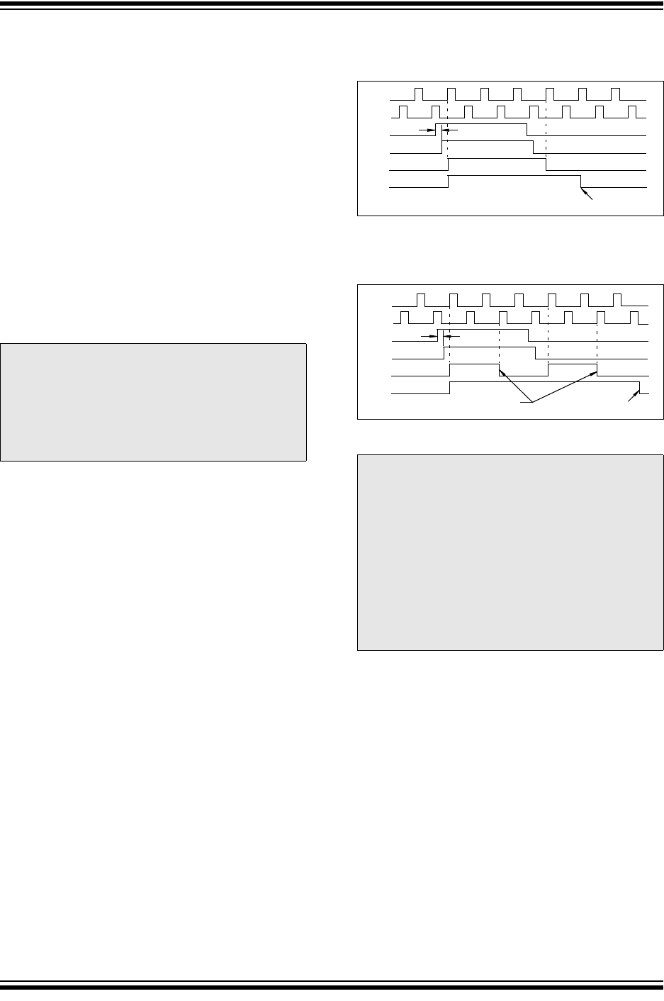
8.4 Comparator Interrupt Operation
The comparator interrupt flag can be set whenever
there is a change in the output value of the comparator.
Changes are recognized by means of a mismatch
circuit which consists of two latches and an exclusive-
or gate (see Figures 8-2 and 8-3). One latch is updated
with the comparator output level when the CMxCON0
register is read. This latch retains the value until the
next read of the CMxCON0 register or the occurrence
of a Reset. The other latch of the mismatch circuit is
updated on every Q1 system clock. A mismatch
condition will occur when a comparator output change
is clocked through the second latch on the Q1 clock
cycle. At this point the two mismatch latches have
opposite output levels which is detected by the
exclusive-or gate and fed to the interrupt circuitry. The
mismatch condition persists until either the CMxCON0
register is read or the comparator output returns to the
previous state.
The comparator interrupt is set by the mismatch edge
and not the mismatch level. This means that the inter-
rupt flag can be reset without the additional step of
reading or writing the CMxCON0 register to clear the
mismatch registers. When the mismatch registers are
cleared, an interrupt will occur upon the comparator’s
return to the previous state, otherwise no interrupt will
be generated.
Software will need to maintain information about the
status of the comparator output, as read from the
CMxCON0 register, or CM2CON1 register, to determine
the actual change that has occurred.
The CxIF bit of the PIR2 register is the comparator
interrupt flag. This bit must be reset in software by
clearing it to ‘0’. Since it is also possible to write a ‘1’ to
this register, an interrupt can be generated.
The CxIE bit of the PIE2 register and the PEIE and GIE
bits of the INTCON register must all be set to enable
comparator interrupts. If any of these bits are cleared,
the interrupt is not enabled, although the CxIF bit of the
PIR2 register will still be set if an interrupt condition
occurs.
FIGURE 8-4: COMPARATOR
INTERRUPT TIMING W/O
CMxCON0 READ
FIGURE 8-5: COMPARATOR
INTERRUPT TIMING WITH
CMxCON0 READ
Note 1: A write operation to the CMxCON0
register will also clear the mismatch
condition because all writes include a read
operation at the beginning of the write
cycle.
2: Comparator interrupts will operate correctly
regardless of the state of CxOE.
Note 1: If a change in the CMxCON0 register
(CxOUT) should occur when a read oper-
ation is being executed (start of the Q2
cycle), then the CxIF of the PIR2 register
interrupt flag may not get set.
2: When either comparator is first enabled,
bias circuitry in the comparator module
may cause an invalid output from the
comparator until the bias circuitry is stable.
Allow about 1 μs for bias settling then clear
the mismatch condition and interrupt flags
before enabling comparator interrupts.
Q1
Q3
C
IN+
CxOUT
Set CxIF (level)
CxIF
TRT
reset by software
Q1
Q3
CxIN+
CxOUT
Set CxIF (level)
CxIF
TRT
reset by software
cleared by CMxCON0 read