
Datasheet


Table Of Contents
- High-Performance RISC CPU:
- Special Microcontroller Features:
- Low-Power Features:
- Peripheral Features:
- Pin Diagrams – PIC16F882/883/886, 28-Pin PDIP, SOIC, SSOP
- Pin Diagrams – PIC16F882/883/886, 28-Pin QFN
- Pin Diagrams – PIC16F884/887, 40-Pin PDIP
- Pin Diagrams – PIC16F884/887, 44-Pin QFN
- Pin Diagrams – PIC16F884/887, 44-Pin TQFP
- Most Current Data Sheet
- Errata
- Customer Notification System
- 1.0 Device Overview
- 2.0 Memory Organization
- 2.1 Program Memory Organization
- 2.2 Data Memory Organization
- 2.2.1 General Purpose Register File
- 2.2.2 Special Function Registers
- FIGURE 2-4: PIC16F882 Special Function Registers
- FIGURE 2-5: PIC16F883/PIC16F884 Special Function Registers
- FIGURE 2-6: PIC16F886/PIC16F887 Special Function Registers
- TABLE 2-1: PIC16F882/883/884/886/887 Special Function Registers Summary Bank 0
- TABLE 2-2: PIC16F882/883/884/886/887 Special Function Registers Summary Bank 1
- TABLE 2-3: PIC16F882/883/884/886/887 Special Function Registers Summary Bank 2
- TABLE 2-4: PIC16F882/883/884/886/887 Special Function Registers Summary Bank 3
- Register 2-1: STATUS: STATUS Register
- Register 2-2: OPTION_REG: OPTION Register
- Register 2-3: INTCON: Interrupt Control Register
- Register 2-4: PIE1: Peripheral Interrupt Enable Register 1
- Register 2-5: PIE2: Peripheral Interrupt Enable Register 2
- Register 2-6: PIR1: Peripheral Interrupt Request Register 1
- Register 2-7: PIR2: Peripheral Interrupt Request Register 2
- Register 2-8: PCON: Power Control Register
- 2.3 PCL and PCLATH
- 2.4 Indirect Addressing, INDF and FSR Registers
- 3.0 I/O Ports
- 3.1 PORTA and the TRISA Registers
- 3.2 Additional Pin Functions
- 3.2.1 ANSEL Register
- 3.2.2 Ultra Low-Power Wake-up
- 3.2.3 Pin Descriptions and Diagrams
- FIGURE 3-1: Block Diagram of RA0
- FIGURE 3-2: Block Diagram of RA1
- FIGURE 3-3: Block Diagram of RA2
- FIGURE 3-4: Block Diagram of RA3
- FIGURE 3-5: Block Diagram of RA4
- FIGURE 3-6: Block Diagram of RA5
- FIGURE 3-7: Block Diagram of RA6
- FIGURE 3-8: Block Diagram of RA7
- TABLE 3-1: Summary of Registers Associated with PORTA
- 3.3 PORTB and TRISB Registers
- 3.4 Additional PORTB Pin Functions
- 3.5 PORTC and TRISC Registers
- 3.6 PORTD and TRISD Registers
- 3.7 PORTE and TRISE Registers
- 4.0 Oscillator Module (With Fail-Safe Clock Monitor)
- 5.0 Timer0 Module
- 6.0 Timer1 Module with Gate Control
- 6.1 Timer1 Operation
- 6.2 Clock Source Selection
- 6.3 Timer1 Prescaler
- 6.4 Timer1 Oscillator
- 6.5 Timer1 Operation in Asynchronous Counter Mode
- 6.6 Timer1 Gate
- 6.7 Timer1 Interrupt
- 6.8 Timer1 Operation During Sleep
- 6.9 ECCP Capture/Compare Time Base
- 6.10 ECCP Special Event Trigger
- 6.11 Comparator Synchronization
- 6.12 Timer1 Control Register
- 7.0 Timer2 Module
- 8.0 Comparator Module
- 8.1 Comparator Overview
- 8.2 Comparator Control
- 8.3 Comparator Response Time
- 8.4 Comparator Interrupt Operation
- 8.5 Operation During Sleep
- 8.6 Effects of a Reset
- 8.7 Analog Input Connection Considerations
- 8.8 Additional Comparator Features
- 8.9 Comparator SR Latch
- 8.10 Comparator Voltage Reference
- 8.10.1 Independent Operation
- 8.10.2 Output Voltage Selection
- 8.10.3 Output Clamped to Vss
- 8.10.4 Output Ratiometric to Vdd
- 8.10.5 Fixed Voltage Reference
- 8.10.6 Fixed Voltage Reference Stabilization Period
- 8.10.7 Voltage Reference Selection
- FIGURE 8-8: Comparator Voltage Reference Block Diagram
- FIGURE 8-9: Comparator and ADC Voltage REference Block Diagram
- TABLE 8-2: Comparator and ADC Voltage Reference Priority
- Register 8-5: VRCON: Voltage Reference Control register
- TABLE 8-3: Summary of Registers Associated with the Comparator and Voltage Reference Modules
- 9.0 Analog-to-Digital Converter (ADC) Module
- FIGURE 9-1: ADC Block Diagram
- 9.1 ADC Configuration
- 9.2 ADC Operation
- 9.2.1 Starting a Conversion
- 9.2.2 Completion of a Conversion
- 9.2.3 Terminating a conversion
- 9.2.4 ADC Operation During Sleep
- 9.2.5 Special Event Trigger
- 9.2.6 A/D Conversion Procedure
- 9.2.7 ADC Register Definitions
- Register 9-1: ADCON0: A/D Control Register 0
- Register 9-2: ADCON1: A/D Control Register 1
- Register 9-3: ADRESH: ADC Result Register High (ADRESH) ADFM = 0
- Register 9-4: ADRESL: ADC Result Register Low (ADRESL) ADFM = 0
- Register 9-5: ADRESH: ADC Result Register High (ADRESH) ADFM = 1
- Register 9-6: ADRESL: ADC Result Register Low (ADRESL) ADFM = 1
- 9.3 A/D Acquisition Requirements
- 10.0 Data EEPROM and Flash Program Memory Control
- 10.1 EEADR and EEADRH Registers
- 10.2 Writing to Flash Program Memory
- 10.3 Write Verify
- 10.4 Protection Against Spurious Write
- 10.5 Data EEPROM Operation During Code-Protect
- 11.0 Capture/Compare/PWM Modules (CCP1 and CCP2)
- 11.1 Enhanced Capture/Compare/PWM (CCP1)
- 11.2 Capture/Compare/PWM (CCP2)
- 11.3 Capture Mode
- 11.4 Compare Mode
- 11.5 PWM Mode
- 11.6 PWM (Enhanced Mode)
- FIGURE 11-5: Example Simplified Block Diagram of the Enhanced PWM Mode
- TABLE 11-5: Example Pin Assignments for Various PWM Enhanced Modes
- FIGURE 11-6: Example PWM (enhanced Mode) Output Relationships (Active-High State)
- FIGURE 11-7: Example Enhanced PWM Output Relationships (Active-Low State)
- 11.6.1 Half-Bridge Mode
- 11.6.2 Full-Bridge Mode
- 11.6.3 Start-up Considerations
- 11.6.4 Enhanced PWM Auto- shutdown mode
- 11.6.5 Auto-Restart Mode
- 11.6.6 Programmable Dead-Band Delay Mode
- 11.6.7 Pulse Steering Mode
- Register 11-5: PSTRCON: Pulse Steering Control Register(1)
- FIGURE 11-19: Simplified Steering Block Diagram
- FIGURE 11-20: Example of Steering Event at End of Instruction (STRSYNC = 0)
- FIGURE 11-21: Example of Steering Event at Beginning of Instruction (STRSYNC = 1)
- TABLE 11-6: Registers Associated with Capture, cOMPARE and Timer1
- TABLE 11-7: Registers Associated with PWM and Timer2
- 12.0 Enhanced Universal Synchronous Asynchronous Receiver Transmitter (EUSART)
- FIGURE 12-1: EUSART Transmit Block Diagram
- FIGURE 12-2: EUSART Receive Block Diagram
- 12.1 EUSART Asynchronous Mode
- 12.2 Clock Accuracy with Asynchronous Operation
- 12.3 EUSART Baud Rate Generator (BRG)
- 12.4 EUSART Synchronous Mode
- 12.5 EUSART Operation During Sleep
- 13.0 Master Synchronous Serial Port (MSSP) Module
- 13.1 Master SSP (MSSP) Module Overview
- 13.2 Control Registers
- 13.3 SPI Mode
- 13.4 MSSP I2C Operation
- FIGURE 13-6: MSSP Block Diagram (I2C Mode)
- 13.4.1 SLAVE Mode
- 13.4.2 General Call Address Support
- 13.4.3 Master Mode
- 13.4.4 I2C™ Master Mode Support
- 13.4.5 Baud Rate Generator
- 13.4.6 I2C™ Master Mode Start Condition Timing
- 13.4.7 I2C™ Master Mode Repeated Start Condition Timing
- 13.4.8 I2C™ Master Mode Transmission
- 13.4.9 I2C™ Master Mode Reception
- 13.4.10 Acknowledge Sequence Timing
- 13.4.11 Stop Condition Timing
- 13.4.12 Clock Arbitration
- 13.4.13 Sleep Operation
- 13.4.14 Effect of a Reset
- 13.4.15 Multi-Master Mode
- 13.4.16 Multi -Master Communication, Bus Collision, and Bus Arbitration
- FIGURE 13-20: Bus Collision Timing for Transmit and Acknowledge
- FIGURE 13-21: Bus Collision During Start Condition (SDA only)
- FIGURE 13-22: Bus Collision During Start Condition (SCL = 0)
- FIGURE 13-23: BRG Reset Due to SDA Arbitration During Start Condition
- FIGURE 13-24: Bus Collision During a Repeated Start Condition (Case 1)
- FIGURE 13-25: Bus Collision During Repeated Start Condition (Case 2)
- FIGURE 13-26: Bus Collision During a Stop Condition (Case 1)
- FIGURE 13-27: Bus Collision During a Stop Condition (Case 2)
- 13.4.17 SSP Mask Register
- 14.0 Special Features of the CPU
- 14.1 Configuration Bits
- 14.2 Reset
- FIGURE 14-1: Simplified Block Diagram of On-chip Reset Circuit
- 14.2.1 Power-on Reset (POR)
- 14.2.2 MCLR
- 14.2.3 Power-up Timer (PWRT)
- 14.2.4 Brown-out Reset (BOR)
- 14.2.5 Time-out Sequence
- 14.2.6 Power Control (PCON) Register
- TABLE 14-1: Time-out in Various Situations
- TABLE 14-2: Status/PCON Bits and Their Significance
- TABLE 14-3: Summary of Registers Associated with Brown-out
- FIGURE 14-4: Time-out Sequence On Power-up (Delayed MCLR): Case 1
- FIGURE 14-5: Time-out Sequence On Power-up (Delayed MCLR): Case 2
- FIGURE 14-6: Time-out Sequence on Power-up (MCLR with Vdd)
- TABLE 14-4: Initialization Condition for Register
- TABLE 14-5: Initialization Condition for Special Registers
- 14.3 Interrupts
- 14.4 Context Saving During Interrupts
- 14.5 Watchdog Timer (WDT)
- 14.6 Power-Down Mode (Sleep)
- 14.7 Code Protection
- 14.8 ID Locations
- 14.9 In-Circuit Serial Programming™
- 14.10 Low-Voltage (Single-Supply) ICSP Programming
- 14.11 In-Circuit Debugger
- 15.0 Instruction Set Summary
- 16.0 Development Support
- 16.1 MPLAB Integrated Development Environment Software
- 16.2 MPASM Assembler
- 16.3 MPLAB C18 and MPLAB C30 C Compilers
- 16.4 MPLINK Object Linker/ MPLIB Object Librarian
- 16.5 MPLAB ASM30 Assembler, Linker and Librarian
- 16.6 MPLAB SIM Software Simulator
- 16.7 MPLAB ICE 2000 High-Performance In-Circuit Emulator
- 16.8 MPLAB REAL ICE In-Circuit Emulator System
- 16.9 MPLAB ICD 2 In-Circuit Debugger
- 16.10 MPLAB PM3 Device Programmer
- 16.11 PICSTART Plus Development Programmer
- 16.12 PICkit 2 Development Programmer
- 16.13 Demonstration, Development and Evaluation Boards
- 17.0 Electrical Specifications
- Absolute Maximum Ratings(†)
- 17.1 DC Characteristics: PIC16F883/884/886/887-I (Industrial) PIC16F883/884/886/887-E (Extended)
- 17.2 DC Characteristics: PIC16F883/884/886/887-I (Industrial) PIC16F883/884/886/887-E (Extended)
- 17.3 DC Characteristics: PIC16F883/884/886/887-I (Industrial)
- 17.4 DC Characteristics: PIC16F883/884/886/887-E (Extended)
- 17.5 DC Characteristics: PIC16F883/884/886/887-I (Industrial) PIC16F883/884/886/887-E (Extended)
- 17.6 Thermal Considerations
- 17.7 Timing Parameter Symbology
- 17.8 AC Characteristics: PIC16F883/884/886/887 (Industrial, Extended)
- FIGURE 17-4: Clock Timing
- TABLE 17-1: Clock Oscillator Timing Requirements
- TABLE 17-2: Oscillator Parameters
- FIGURE 17-5: CLKOUT and I/O Timing
- TABLE 17-3: CLKOUT and I/O Timing Parameters
- FIGURE 17-6: Reset, Watchdog Timer, Oscillator Start-up Timer and Power-up Timer Timing
- FIGURE 17-7: Brown-out Reset Timing and Characteristics
- TABLE 17-4: Reset, Watchdog Timer, Oscillator Start-up Timer, Power-up Timer and Brown-out Reset Parameters
- FIGURE 17-8: Timer0 and Timer1 External Clock Timings
- TABLE 17-5: Timer0 and Timer1 External Clock Requirements
- FIGURE 17-9: Capture/Compare/PWM Timings (ECCP)
- TABLE 17-6: Capture/Compare/PWM Requirements (ECCP)
- TABLE 17-7: Comparator Specifications
- TABLE 17-8: Comparator Voltage Reference (CVref) Specifications
- TABLE 17-9: Voltage (VR) Reference Specifications
- TABLE 17-10: PIC16F883/884/886/887 A/D Converter (ADC) Characteristics
- TABLE 17-11: PIC16F883/884/886/887 A/D Conversion Requirements
- FIGURE 17-10: PIC16F883/884/886/887 A/D Conversion Timing (Normal Mode)
- FIGURE 17-11: PIC16F883/884/886/887 A/D Conversion Timing (Sleep Mode)
- FIGURE 17-12: EUSART Synchronous Transmission (Master/Slave) Timing
- TABLE 17-12: EUSART Synchronous Transmission Requirements
- FIGURE 17-13: EUSART Synchronous Receive (Master/Slave) Timing
- TABLE 17-13: EUSART Synchronous Receive Requirements
- FIGURE 17-14: SPI Master Mode Timing (CKE = 0, smp = 0)
- FIGURE 17-15: SPI Master Mode Timing (CKE = 1, SMP = 1)
- FIGURE 17-16: SPI Slave Mode Timing (CKE = 0)
- FIGURE 17-17: SPI Slave Mode Timing (CKE = 1)
- TABLE 17-14: SPI Mode requirements
- FIGURE 17-18: I2C™ Bus Start/Stop Bits Timing
- TABLE 17-15: I2C™ Bus Start/Stop Bits Requirements
- FIGURE 17-19: I2C™ Bus Data Timing
- TABLE 17-16: I2C™ Bus Data Requirements
- 18.0 DC and AC Characteristics Graphs and Tables
- FIGURE 18-1: Typical Idd vs. Fosc Over Vdd (EC Mode)
- FIGURE 18-2: Maximum Idd vs. Fosc Over Vdd (EC Mode)
- FIGURE 18-3: Typical Idd vs. Fosc Over Vdd (HS Mode)
- FIGURE 18-4: Maximum Idd vs. Fosc Over Vdd (HS Mode)
- FIGURE 18-5: Typical Idd vs. Vdd Over Fosc (XT Mode)
- FIGURE 18-6: Maximum Idd vs. Vdd Over Fosc (XT Mode)
- FIGURE 18-7: Typical Idd vs. Vdd Over Fosc (EXTRC Mode)
- FIGURE 18-8: Maximum Idd vs. Vdd (EXTRC Mode)
- FIGURE 18-9: Idd vs. Vdd Over Fosc (LFINTOSC Mode, 31 kHz)
- FIGURE 18-10: Idd vs. Vdd (LP Mode)
- FIGURE 18-11: Typical Idd vs. Fosc Over Vdd (HFINTOSC Mode)
- FIGURE 18-12: Maximum Idd vs. Fosc Over Vdd (HFINTOSC Mode)
- FIGURE 18-13: Typical Ipd vs. Vdd (Sleep Mode, all Peripherals Disabled)
- FIGURE 18-14: Maximum Ipd vs. Vdd (Sleep Mode, all Peripherals Disabled)
- FIGURE 18-15: Comparator Ipd vs. Vdd (Both Comparators Enabled)
- FIGURE 18-16: BOR Ipd VS. Vdd Over Temperature
- FIGURE 18-17: Typical WDT Ipd VS. Vdd (25°C)
- FIGURE 18-18: Maximum WDT Ipd VS. Vdd Over Temperature
- FIGURE 18-19: WDT Period VS. Vdd Over Temperature
- FIGURE 18-20: WDT Period VS. Temperature (Vdd = 5.0V)
- FIGURE 18-21: CVref Ipd VS. Vdd Over Temperature (High Range)
- FIGURE 18-22: CVref Ipd VS. Vdd Over Temperature (Low Range)
- FIGURE 18-23: Typical VP6 Reference Ipd vs. Vdd (25°C)
- FIGURE 18-24: Maximum VP6 Reference Ipd vs. Vdd Over Temperature
- FIGURE 18-25: T1OSC Ipd vs. Vdd Over Temperature (32 kHz)
- FIGURE 18-26: Vol VS. Iol Over Temperature (Vdd = 3.0V)
- FIGURE 18-27: Vol VS. Iol Over Temperature (Vdd = 5.0V)
- FIGURE 18-28: Voh VS. Ioh Over Temperature (Vdd = 3.0V)
- FIGURE 18-29: Voh VS. Ioh Over Temperature (Vdd = 5.0V)
- FIGURE 18-30: TTL Input Threshold Vin VS. Vdd Over Temperature
- FIGURE 18-31: Schmitt Trigger Input Threshold Vin VS. Vdd Over Temperature
- FIGURE 18-32: Comparator Response Time (Rising Edge)
- FIGURE 18-33: Comparator Response Time (Falling Edge)
- FIGURE 18-34: LFINTOSC Frequency vs. Vdd Over Temperature (31 kHz)
- FIGURE 18-35: ADC Clock Period vs. Vdd Over Temperature
- FIGURE 18-36: Typical HFINTOSC Start-Up Times vs. Vdd Over Temperature
- FIGURE 18-37: Maximum HFINTOSC Start-Up Times vs. Vdd Over Temperature
- FIGURE 18-38: Minimum HFINTOSC Start-Up Times vs. Vdd Over Temperature
- FIGURE 18-39: Typical HFINTOSC Frequency Change vs. Vdd (25°C)
- FIGURE 18-40: Typical HFINTOSC Frequency Change Over Device Vdd (85°C)
- FIGURE 18-41: Typical HFINTOSC Frequency Change vs. Vdd (125°C)
- FIGURE 18-42: Typical HFINTOSC Frequency Change vs. Vdd (-40°C)
- FIGURE 18-43: Typical VP6 Reference Voltage vs. Vdd (25°C)
- FIGURE 18-44: VP6 Drift Over Temperature Normalized at 25°C (Vdd 5V)
- FIGURE 18-45: VP6 Drift Over Temperature Normalized at 25°C (Vdd 3V)
- FIGURE 18-46: Typical VP6 Reference Voltage Distribution (3V, 25°C)
- FIGURE 18-47: Typical VP6 Reference Voltage Distribution (3V, 85°C)
- FIGURE 18-48: Typical VP6 Reference Voltage Distribution (3V, 125°C)
- FIGURE 18-49: Typical VP6 Reference Voltage Distribution (3V, -40°C)
- FIGURE 18-50: Typical VP6 Reference Voltage Distribution (5V, 25°C)
- FIGURE 18-51: Typical VP6 Reference Voltage Distribution (5V, 85°C)
- FIGURE 18-52: Typical VP6 Reference Voltage Distribution (5V, 125°C)
- FIGURE 18-53: Typical VP6 Reference Voltage Distribution (5V, -40°C)
- 19.0 Packaging Information
- Appendix A: Data Sheet Revision History
- Appendix B: Migrating from other PIC® Devices
- INDEX
- The Microchip Web Site
- Customer Change Notification Service
- Customer Support
- Reader Response
- Product ID
- Worldwide Sales
PIC16F882/883/884/886/887
DS41291F-page 26 © 2009 Microchip Technology Inc.
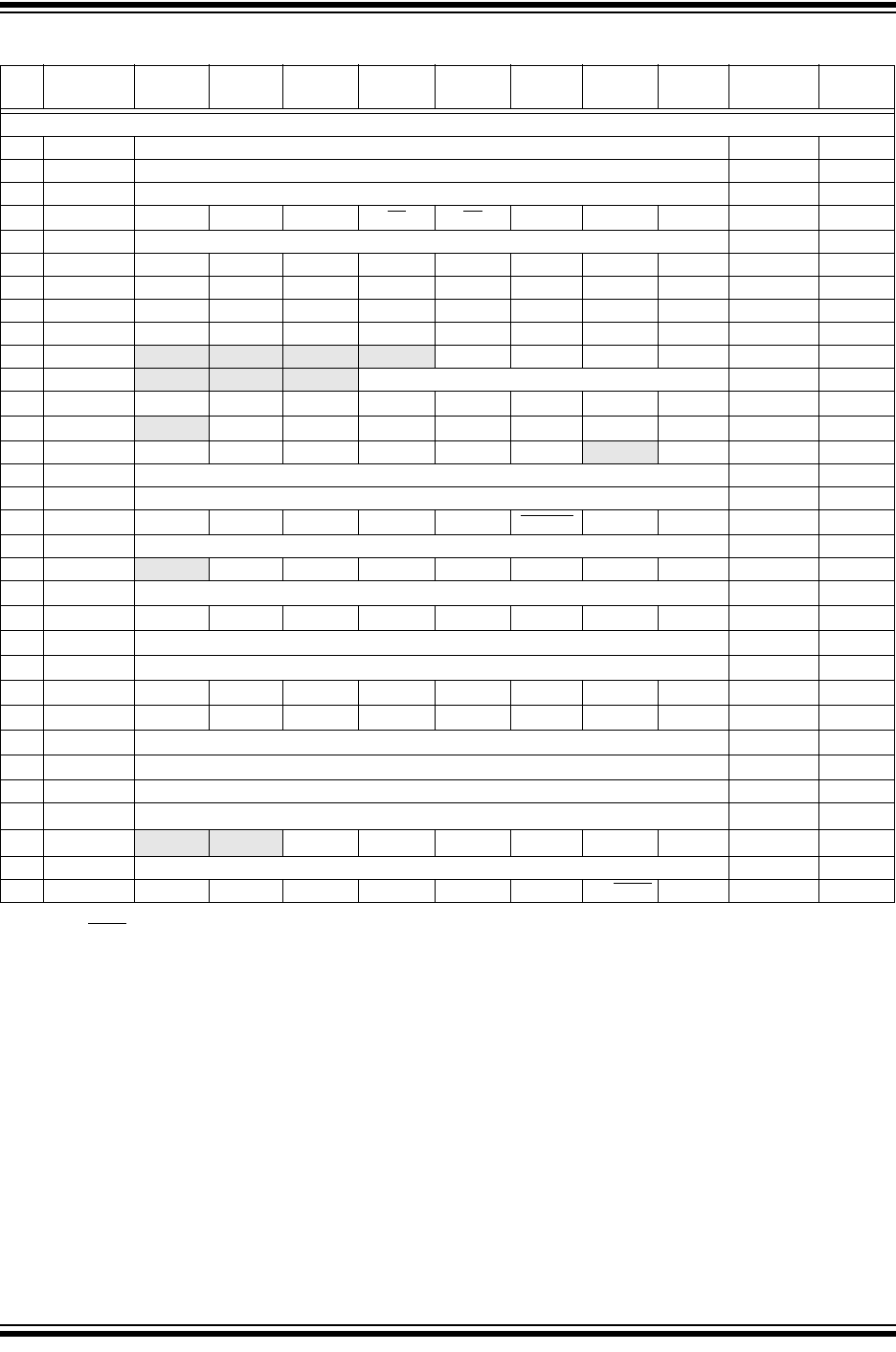
TABLE 2-1: PIC16F882/883/884/886/887 SPECIAL FUNCTION REGISTERS SUMMARY BANK 0
Addr Name Bit 7 Bit 6 Bit 5 Bit 4 Bit 3 Bit 2 Bit 1 Bit 0
Value on
POR, BOR
Page
Bank 0
00h INDF Addressing this location uses contents of FSR to address data memory (not a physical register) xxxx xxxx 37,217
01h TMR0 Timer0 Module Register xxxx xxxx 73,217
02h PCL Program Counter’s (PC) Least Significant Byte 0000 0000 37,217
03h STATUS IRP RP1 RP0 TO
PD ZDCC0001 1xxx 29,217
04h FSR Indirect Data Memory Address Pointer xxxx xxxx 37,217
05h PORTA
(3)
RA7 RA6 RA5 RA4 RA3 RA2 RA1 RA0 xxxx xxxx 39,217
06h PORTB
(3)
RB7 RB6 RB5 RB4 RB3 RB2 RB1 RB0 xxxx xxxx 48,217
07h PORTC
(3)
RC7 RC6 RC5 RC4 RC3 RC2 RC1 RC0 xxxx xxxx 53,217
08h PORTD
(3,4)
RD7 RD6 RD5 RD4 RD3 RD2 RD1 RD0 xxxx xxxx 57,217
09h PORTE
(3)
— — — —RE3RE2
(4)
RE1
(4)
RE0
(4)
---- xxxx 59,217
0Ah PCLATH
— — — Write Buffer for upper 5 bits of Program Counter ---0 0000 37,217
0Bh INTCON GIE PEIE T0IE INTE RBIE T0IF INTF RBIF
(1)
0000 000x 31,217
0Ch PIR1
— ADIF RCIF TXIF SSPIF CCP1IF TMR2IF TMR1IF -000 0000 34,217
0Dh PIR2
OSFIF C2IF C1IF EEIF BCLIF ULPWUIF —CCP2IF0000 00-0 35,217
0Eh TMR1L Holding Register for the Least Significant Byte of the 16-bit TMR1 Register xxxx xxxx 76,217
0Fh TMR1H Holding Register for the Most Significant Byte of the 16-bit TMR1 Register xxxx xxxx 76,217
10h T1CON
T1GINV TMR1GE T1CKPS1 T1CKPS0 T1OSCEN T1SYNC TMR1CS TMR1ON 0000 0000 79,217
11h TMR2 Timer2 Module Register 0000 0000 81,217
12h T2CON
— TOUTPS3 TOUTPS2 TOUTPS1 TOUTPS0 TMR2ON T2CKPS1 T2CKPS0 -000 0000 82,217
13h SSPBUF Synchronous Serial Port Receive Buffer/Transmit Register xxxx xxxx 183,217
14h SSPCON
(2)
WCOL SSPOV SSPEN CKP SSPM3 SSPM2 SSPM1 SSPM0 0000 0000 181,217
15h CCPR1L Capture/Compare/PWM Register 1 Low Byte (LSB) xxxx xxxx 126,217
16h CCPR1H Capture/Compare/PWM Register 1 High Byte (MSB) xxxx xxxx 126,217
17h CCP1CON P1M1 P1M0 DC1B1 DC1B0 CCP1M3 CCP1M2 CCP1M1 CCP1M0 0000 0000 124,217
18h RCSTA SPEN RX9 SREN CREN ADDEN FERR OERR RX9D 0000 000x 161,217
19h TXREG EUSART Transmit Data Register 0000 0000 153,217
1Ah RCREG EUSART Receive Data Register 0000 0000 158,217
1Bh CCPR2L Capture/Compare/PWM Register 2 Low Byte (LSB) xxxx xxxx 126,217
1Ch
CCPR2H Capture/Compare/PWM Register 2 High Byte (MSB) xxxx xxxx
126,218
1Dh
CCP2CON
— —
DC2B1 DC2B0 CCP2M3 CCP2M2 CCP2M1 CCP2M0 --00 0000 125,218
1Eh ADRESH A/D Result Register High Byte xxxx xxxx 99,218
1Fh ADCON0 ADCS1 ADCS0 CHS3 CHS2 CHS1 CHS0 GO/DONE
ADON 0000 0000 104,218
Legend: – = Unimplemented locations read as ‘0’, u = unchanged, x = unknown, q = value depends on condition, shaded = unimplemented
Note 1: MCLR
and WDT Reset do not affect the previous value data latch. The RBIF bit will be cleared upon Reset but will set again if the
mismatch exists.
2: When SSPCON register bits SSPM<3:0> = 1001, any reads or writes to the SSPADD SFR address are accessed through the SSPMSK
register. See Registers • and 13-4 for more detail.
3: Port pins with analog functions controlled by the ANSEL and ANSELH registers will read ‘0’ immediately after a Reset even though the
data latches are either undefined (POR) or unchanged (other Resets).
4: PIC16F884/PIC16F887 only.