
Datasheet


Table Of Contents
- High-Performance RISC CPU:
- Special Microcontroller Features:
- Low-Power Features:
- Peripheral Features:
- Pin Diagrams – PIC16F882/883/886, 28-Pin PDIP, SOIC, SSOP
- Pin Diagrams – PIC16F882/883/886, 28-Pin QFN
- Pin Diagrams – PIC16F884/887, 40-Pin PDIP
- Pin Diagrams – PIC16F884/887, 44-Pin QFN
- Pin Diagrams – PIC16F884/887, 44-Pin TQFP
- Most Current Data Sheet
- Errata
- Customer Notification System
- 1.0 Device Overview
- 2.0 Memory Organization
- 2.1 Program Memory Organization
- 2.2 Data Memory Organization
- 2.2.1 General Purpose Register File
- 2.2.2 Special Function Registers
- FIGURE 2-4: PIC16F882 Special Function Registers
- FIGURE 2-5: PIC16F883/PIC16F884 Special Function Registers
- FIGURE 2-6: PIC16F886/PIC16F887 Special Function Registers
- TABLE 2-1: PIC16F882/883/884/886/887 Special Function Registers Summary Bank 0
- TABLE 2-2: PIC16F882/883/884/886/887 Special Function Registers Summary Bank 1
- TABLE 2-3: PIC16F882/883/884/886/887 Special Function Registers Summary Bank 2
- TABLE 2-4: PIC16F882/883/884/886/887 Special Function Registers Summary Bank 3
- Register 2-1: STATUS: STATUS Register
- Register 2-2: OPTION_REG: OPTION Register
- Register 2-3: INTCON: Interrupt Control Register
- Register 2-4: PIE1: Peripheral Interrupt Enable Register 1
- Register 2-5: PIE2: Peripheral Interrupt Enable Register 2
- Register 2-6: PIR1: Peripheral Interrupt Request Register 1
- Register 2-7: PIR2: Peripheral Interrupt Request Register 2
- Register 2-8: PCON: Power Control Register
- 2.3 PCL and PCLATH
- 2.4 Indirect Addressing, INDF and FSR Registers
- 3.0 I/O Ports
- 3.1 PORTA and the TRISA Registers
- 3.2 Additional Pin Functions
- 3.2.1 ANSEL Register
- 3.2.2 Ultra Low-Power Wake-up
- 3.2.3 Pin Descriptions and Diagrams
- FIGURE 3-1: Block Diagram of RA0
- FIGURE 3-2: Block Diagram of RA1
- FIGURE 3-3: Block Diagram of RA2
- FIGURE 3-4: Block Diagram of RA3
- FIGURE 3-5: Block Diagram of RA4
- FIGURE 3-6: Block Diagram of RA5
- FIGURE 3-7: Block Diagram of RA6
- FIGURE 3-8: Block Diagram of RA7
- TABLE 3-1: Summary of Registers Associated with PORTA
- 3.3 PORTB and TRISB Registers
- 3.4 Additional PORTB Pin Functions
- 3.5 PORTC and TRISC Registers
- 3.6 PORTD and TRISD Registers
- 3.7 PORTE and TRISE Registers
- 4.0 Oscillator Module (With Fail-Safe Clock Monitor)
- 5.0 Timer0 Module
- 6.0 Timer1 Module with Gate Control
- 6.1 Timer1 Operation
- 6.2 Clock Source Selection
- 6.3 Timer1 Prescaler
- 6.4 Timer1 Oscillator
- 6.5 Timer1 Operation in Asynchronous Counter Mode
- 6.6 Timer1 Gate
- 6.7 Timer1 Interrupt
- 6.8 Timer1 Operation During Sleep
- 6.9 ECCP Capture/Compare Time Base
- 6.10 ECCP Special Event Trigger
- 6.11 Comparator Synchronization
- 6.12 Timer1 Control Register
- 7.0 Timer2 Module
- 8.0 Comparator Module
- 8.1 Comparator Overview
- 8.2 Comparator Control
- 8.3 Comparator Response Time
- 8.4 Comparator Interrupt Operation
- 8.5 Operation During Sleep
- 8.6 Effects of a Reset
- 8.7 Analog Input Connection Considerations
- 8.8 Additional Comparator Features
- 8.9 Comparator SR Latch
- 8.10 Comparator Voltage Reference
- 8.10.1 Independent Operation
- 8.10.2 Output Voltage Selection
- 8.10.3 Output Clamped to Vss
- 8.10.4 Output Ratiometric to Vdd
- 8.10.5 Fixed Voltage Reference
- 8.10.6 Fixed Voltage Reference Stabilization Period
- 8.10.7 Voltage Reference Selection
- FIGURE 8-8: Comparator Voltage Reference Block Diagram
- FIGURE 8-9: Comparator and ADC Voltage REference Block Diagram
- TABLE 8-2: Comparator and ADC Voltage Reference Priority
- Register 8-5: VRCON: Voltage Reference Control register
- TABLE 8-3: Summary of Registers Associated with the Comparator and Voltage Reference Modules
- 9.0 Analog-to-Digital Converter (ADC) Module
- FIGURE 9-1: ADC Block Diagram
- 9.1 ADC Configuration
- 9.2 ADC Operation
- 9.2.1 Starting a Conversion
- 9.2.2 Completion of a Conversion
- 9.2.3 Terminating a conversion
- 9.2.4 ADC Operation During Sleep
- 9.2.5 Special Event Trigger
- 9.2.6 A/D Conversion Procedure
- 9.2.7 ADC Register Definitions
- Register 9-1: ADCON0: A/D Control Register 0
- Register 9-2: ADCON1: A/D Control Register 1
- Register 9-3: ADRESH: ADC Result Register High (ADRESH) ADFM = 0
- Register 9-4: ADRESL: ADC Result Register Low (ADRESL) ADFM = 0
- Register 9-5: ADRESH: ADC Result Register High (ADRESH) ADFM = 1
- Register 9-6: ADRESL: ADC Result Register Low (ADRESL) ADFM = 1
- 9.3 A/D Acquisition Requirements
- 10.0 Data EEPROM and Flash Program Memory Control
- 10.1 EEADR and EEADRH Registers
- 10.2 Writing to Flash Program Memory
- 10.3 Write Verify
- 10.4 Protection Against Spurious Write
- 10.5 Data EEPROM Operation During Code-Protect
- 11.0 Capture/Compare/PWM Modules (CCP1 and CCP2)
- 11.1 Enhanced Capture/Compare/PWM (CCP1)
- 11.2 Capture/Compare/PWM (CCP2)
- 11.3 Capture Mode
- 11.4 Compare Mode
- 11.5 PWM Mode
- 11.6 PWM (Enhanced Mode)
- FIGURE 11-5: Example Simplified Block Diagram of the Enhanced PWM Mode
- TABLE 11-5: Example Pin Assignments for Various PWM Enhanced Modes
- FIGURE 11-6: Example PWM (enhanced Mode) Output Relationships (Active-High State)
- FIGURE 11-7: Example Enhanced PWM Output Relationships (Active-Low State)
- 11.6.1 Half-Bridge Mode
- 11.6.2 Full-Bridge Mode
- 11.6.3 Start-up Considerations
- 11.6.4 Enhanced PWM Auto- shutdown mode
- 11.6.5 Auto-Restart Mode
- 11.6.6 Programmable Dead-Band Delay Mode
- 11.6.7 Pulse Steering Mode
- Register 11-5: PSTRCON: Pulse Steering Control Register(1)
- FIGURE 11-19: Simplified Steering Block Diagram
- FIGURE 11-20: Example of Steering Event at End of Instruction (STRSYNC = 0)
- FIGURE 11-21: Example of Steering Event at Beginning of Instruction (STRSYNC = 1)
- TABLE 11-6: Registers Associated with Capture, cOMPARE and Timer1
- TABLE 11-7: Registers Associated with PWM and Timer2
- 12.0 Enhanced Universal Synchronous Asynchronous Receiver Transmitter (EUSART)
- FIGURE 12-1: EUSART Transmit Block Diagram
- FIGURE 12-2: EUSART Receive Block Diagram
- 12.1 EUSART Asynchronous Mode
- 12.2 Clock Accuracy with Asynchronous Operation
- 12.3 EUSART Baud Rate Generator (BRG)
- 12.4 EUSART Synchronous Mode
- 12.5 EUSART Operation During Sleep
- 13.0 Master Synchronous Serial Port (MSSP) Module
- 13.1 Master SSP (MSSP) Module Overview
- 13.2 Control Registers
- 13.3 SPI Mode
- 13.4 MSSP I2C Operation
- FIGURE 13-6: MSSP Block Diagram (I2C Mode)
- 13.4.1 SLAVE Mode
- 13.4.2 General Call Address Support
- 13.4.3 Master Mode
- 13.4.4 I2C™ Master Mode Support
- 13.4.5 Baud Rate Generator
- 13.4.6 I2C™ Master Mode Start Condition Timing
- 13.4.7 I2C™ Master Mode Repeated Start Condition Timing
- 13.4.8 I2C™ Master Mode Transmission
- 13.4.9 I2C™ Master Mode Reception
- 13.4.10 Acknowledge Sequence Timing
- 13.4.11 Stop Condition Timing
- 13.4.12 Clock Arbitration
- 13.4.13 Sleep Operation
- 13.4.14 Effect of a Reset
- 13.4.15 Multi-Master Mode
- 13.4.16 Multi -Master Communication, Bus Collision, and Bus Arbitration
- FIGURE 13-20: Bus Collision Timing for Transmit and Acknowledge
- FIGURE 13-21: Bus Collision During Start Condition (SDA only)
- FIGURE 13-22: Bus Collision During Start Condition (SCL = 0)
- FIGURE 13-23: BRG Reset Due to SDA Arbitration During Start Condition
- FIGURE 13-24: Bus Collision During a Repeated Start Condition (Case 1)
- FIGURE 13-25: Bus Collision During Repeated Start Condition (Case 2)
- FIGURE 13-26: Bus Collision During a Stop Condition (Case 1)
- FIGURE 13-27: Bus Collision During a Stop Condition (Case 2)
- 13.4.17 SSP Mask Register
- 14.0 Special Features of the CPU
- 14.1 Configuration Bits
- 14.2 Reset
- FIGURE 14-1: Simplified Block Diagram of On-chip Reset Circuit
- 14.2.1 Power-on Reset (POR)
- 14.2.2 MCLR
- 14.2.3 Power-up Timer (PWRT)
- 14.2.4 Brown-out Reset (BOR)
- 14.2.5 Time-out Sequence
- 14.2.6 Power Control (PCON) Register
- TABLE 14-1: Time-out in Various Situations
- TABLE 14-2: Status/PCON Bits and Their Significance
- TABLE 14-3: Summary of Registers Associated with Brown-out
- FIGURE 14-4: Time-out Sequence On Power-up (Delayed MCLR): Case 1
- FIGURE 14-5: Time-out Sequence On Power-up (Delayed MCLR): Case 2
- FIGURE 14-6: Time-out Sequence on Power-up (MCLR with Vdd)
- TABLE 14-4: Initialization Condition for Register
- TABLE 14-5: Initialization Condition for Special Registers
- 14.3 Interrupts
- 14.4 Context Saving During Interrupts
- 14.5 Watchdog Timer (WDT)
- 14.6 Power-Down Mode (Sleep)
- 14.7 Code Protection
- 14.8 ID Locations
- 14.9 In-Circuit Serial Programming™
- 14.10 Low-Voltage (Single-Supply) ICSP Programming
- 14.11 In-Circuit Debugger
- 15.0 Instruction Set Summary
- 16.0 Development Support
- 16.1 MPLAB Integrated Development Environment Software
- 16.2 MPASM Assembler
- 16.3 MPLAB C18 and MPLAB C30 C Compilers
- 16.4 MPLINK Object Linker/ MPLIB Object Librarian
- 16.5 MPLAB ASM30 Assembler, Linker and Librarian
- 16.6 MPLAB SIM Software Simulator
- 16.7 MPLAB ICE 2000 High-Performance In-Circuit Emulator
- 16.8 MPLAB REAL ICE In-Circuit Emulator System
- 16.9 MPLAB ICD 2 In-Circuit Debugger
- 16.10 MPLAB PM3 Device Programmer
- 16.11 PICSTART Plus Development Programmer
- 16.12 PICkit 2 Development Programmer
- 16.13 Demonstration, Development and Evaluation Boards
- 17.0 Electrical Specifications
- Absolute Maximum Ratings(†)
- 17.1 DC Characteristics: PIC16F883/884/886/887-I (Industrial) PIC16F883/884/886/887-E (Extended)
- 17.2 DC Characteristics: PIC16F883/884/886/887-I (Industrial) PIC16F883/884/886/887-E (Extended)
- 17.3 DC Characteristics: PIC16F883/884/886/887-I (Industrial)
- 17.4 DC Characteristics: PIC16F883/884/886/887-E (Extended)
- 17.5 DC Characteristics: PIC16F883/884/886/887-I (Industrial) PIC16F883/884/886/887-E (Extended)
- 17.6 Thermal Considerations
- 17.7 Timing Parameter Symbology
- 17.8 AC Characteristics: PIC16F883/884/886/887 (Industrial, Extended)
- FIGURE 17-4: Clock Timing
- TABLE 17-1: Clock Oscillator Timing Requirements
- TABLE 17-2: Oscillator Parameters
- FIGURE 17-5: CLKOUT and I/O Timing
- TABLE 17-3: CLKOUT and I/O Timing Parameters
- FIGURE 17-6: Reset, Watchdog Timer, Oscillator Start-up Timer and Power-up Timer Timing
- FIGURE 17-7: Brown-out Reset Timing and Characteristics
- TABLE 17-4: Reset, Watchdog Timer, Oscillator Start-up Timer, Power-up Timer and Brown-out Reset Parameters
- FIGURE 17-8: Timer0 and Timer1 External Clock Timings
- TABLE 17-5: Timer0 and Timer1 External Clock Requirements
- FIGURE 17-9: Capture/Compare/PWM Timings (ECCP)
- TABLE 17-6: Capture/Compare/PWM Requirements (ECCP)
- TABLE 17-7: Comparator Specifications
- TABLE 17-8: Comparator Voltage Reference (CVref) Specifications
- TABLE 17-9: Voltage (VR) Reference Specifications
- TABLE 17-10: PIC16F883/884/886/887 A/D Converter (ADC) Characteristics
- TABLE 17-11: PIC16F883/884/886/887 A/D Conversion Requirements
- FIGURE 17-10: PIC16F883/884/886/887 A/D Conversion Timing (Normal Mode)
- FIGURE 17-11: PIC16F883/884/886/887 A/D Conversion Timing (Sleep Mode)
- FIGURE 17-12: EUSART Synchronous Transmission (Master/Slave) Timing
- TABLE 17-12: EUSART Synchronous Transmission Requirements
- FIGURE 17-13: EUSART Synchronous Receive (Master/Slave) Timing
- TABLE 17-13: EUSART Synchronous Receive Requirements
- FIGURE 17-14: SPI Master Mode Timing (CKE = 0, smp = 0)
- FIGURE 17-15: SPI Master Mode Timing (CKE = 1, SMP = 1)
- FIGURE 17-16: SPI Slave Mode Timing (CKE = 0)
- FIGURE 17-17: SPI Slave Mode Timing (CKE = 1)
- TABLE 17-14: SPI Mode requirements
- FIGURE 17-18: I2C™ Bus Start/Stop Bits Timing
- TABLE 17-15: I2C™ Bus Start/Stop Bits Requirements
- FIGURE 17-19: I2C™ Bus Data Timing
- TABLE 17-16: I2C™ Bus Data Requirements
- 18.0 DC and AC Characteristics Graphs and Tables
- FIGURE 18-1: Typical Idd vs. Fosc Over Vdd (EC Mode)
- FIGURE 18-2: Maximum Idd vs. Fosc Over Vdd (EC Mode)
- FIGURE 18-3: Typical Idd vs. Fosc Over Vdd (HS Mode)
- FIGURE 18-4: Maximum Idd vs. Fosc Over Vdd (HS Mode)
- FIGURE 18-5: Typical Idd vs. Vdd Over Fosc (XT Mode)
- FIGURE 18-6: Maximum Idd vs. Vdd Over Fosc (XT Mode)
- FIGURE 18-7: Typical Idd vs. Vdd Over Fosc (EXTRC Mode)
- FIGURE 18-8: Maximum Idd vs. Vdd (EXTRC Mode)
- FIGURE 18-9: Idd vs. Vdd Over Fosc (LFINTOSC Mode, 31 kHz)
- FIGURE 18-10: Idd vs. Vdd (LP Mode)
- FIGURE 18-11: Typical Idd vs. Fosc Over Vdd (HFINTOSC Mode)
- FIGURE 18-12: Maximum Idd vs. Fosc Over Vdd (HFINTOSC Mode)
- FIGURE 18-13: Typical Ipd vs. Vdd (Sleep Mode, all Peripherals Disabled)
- FIGURE 18-14: Maximum Ipd vs. Vdd (Sleep Mode, all Peripherals Disabled)
- FIGURE 18-15: Comparator Ipd vs. Vdd (Both Comparators Enabled)
- FIGURE 18-16: BOR Ipd VS. Vdd Over Temperature
- FIGURE 18-17: Typical WDT Ipd VS. Vdd (25°C)
- FIGURE 18-18: Maximum WDT Ipd VS. Vdd Over Temperature
- FIGURE 18-19: WDT Period VS. Vdd Over Temperature
- FIGURE 18-20: WDT Period VS. Temperature (Vdd = 5.0V)
- FIGURE 18-21: CVref Ipd VS. Vdd Over Temperature (High Range)
- FIGURE 18-22: CVref Ipd VS. Vdd Over Temperature (Low Range)
- FIGURE 18-23: Typical VP6 Reference Ipd vs. Vdd (25°C)
- FIGURE 18-24: Maximum VP6 Reference Ipd vs. Vdd Over Temperature
- FIGURE 18-25: T1OSC Ipd vs. Vdd Over Temperature (32 kHz)
- FIGURE 18-26: Vol VS. Iol Over Temperature (Vdd = 3.0V)
- FIGURE 18-27: Vol VS. Iol Over Temperature (Vdd = 5.0V)
- FIGURE 18-28: Voh VS. Ioh Over Temperature (Vdd = 3.0V)
- FIGURE 18-29: Voh VS. Ioh Over Temperature (Vdd = 5.0V)
- FIGURE 18-30: TTL Input Threshold Vin VS. Vdd Over Temperature
- FIGURE 18-31: Schmitt Trigger Input Threshold Vin VS. Vdd Over Temperature
- FIGURE 18-32: Comparator Response Time (Rising Edge)
- FIGURE 18-33: Comparator Response Time (Falling Edge)
- FIGURE 18-34: LFINTOSC Frequency vs. Vdd Over Temperature (31 kHz)
- FIGURE 18-35: ADC Clock Period vs. Vdd Over Temperature
- FIGURE 18-36: Typical HFINTOSC Start-Up Times vs. Vdd Over Temperature
- FIGURE 18-37: Maximum HFINTOSC Start-Up Times vs. Vdd Over Temperature
- FIGURE 18-38: Minimum HFINTOSC Start-Up Times vs. Vdd Over Temperature
- FIGURE 18-39: Typical HFINTOSC Frequency Change vs. Vdd (25°C)
- FIGURE 18-40: Typical HFINTOSC Frequency Change Over Device Vdd (85°C)
- FIGURE 18-41: Typical HFINTOSC Frequency Change vs. Vdd (125°C)
- FIGURE 18-42: Typical HFINTOSC Frequency Change vs. Vdd (-40°C)
- FIGURE 18-43: Typical VP6 Reference Voltage vs. Vdd (25°C)
- FIGURE 18-44: VP6 Drift Over Temperature Normalized at 25°C (Vdd 5V)
- FIGURE 18-45: VP6 Drift Over Temperature Normalized at 25°C (Vdd 3V)
- FIGURE 18-46: Typical VP6 Reference Voltage Distribution (3V, 25°C)
- FIGURE 18-47: Typical VP6 Reference Voltage Distribution (3V, 85°C)
- FIGURE 18-48: Typical VP6 Reference Voltage Distribution (3V, 125°C)
- FIGURE 18-49: Typical VP6 Reference Voltage Distribution (3V, -40°C)
- FIGURE 18-50: Typical VP6 Reference Voltage Distribution (5V, 25°C)
- FIGURE 18-51: Typical VP6 Reference Voltage Distribution (5V, 85°C)
- FIGURE 18-52: Typical VP6 Reference Voltage Distribution (5V, 125°C)
- FIGURE 18-53: Typical VP6 Reference Voltage Distribution (5V, -40°C)
- 19.0 Packaging Information
- Appendix A: Data Sheet Revision History
- Appendix B: Migrating from other PIC® Devices
- INDEX
- The Microchip Web Site
- Customer Change Notification Service
- Customer Support
- Reader Response
- Product ID
- Worldwide Sales
© 2009 Microchip Technology Inc. DS41291F-page 219
PIC16F882/883/884/886/887
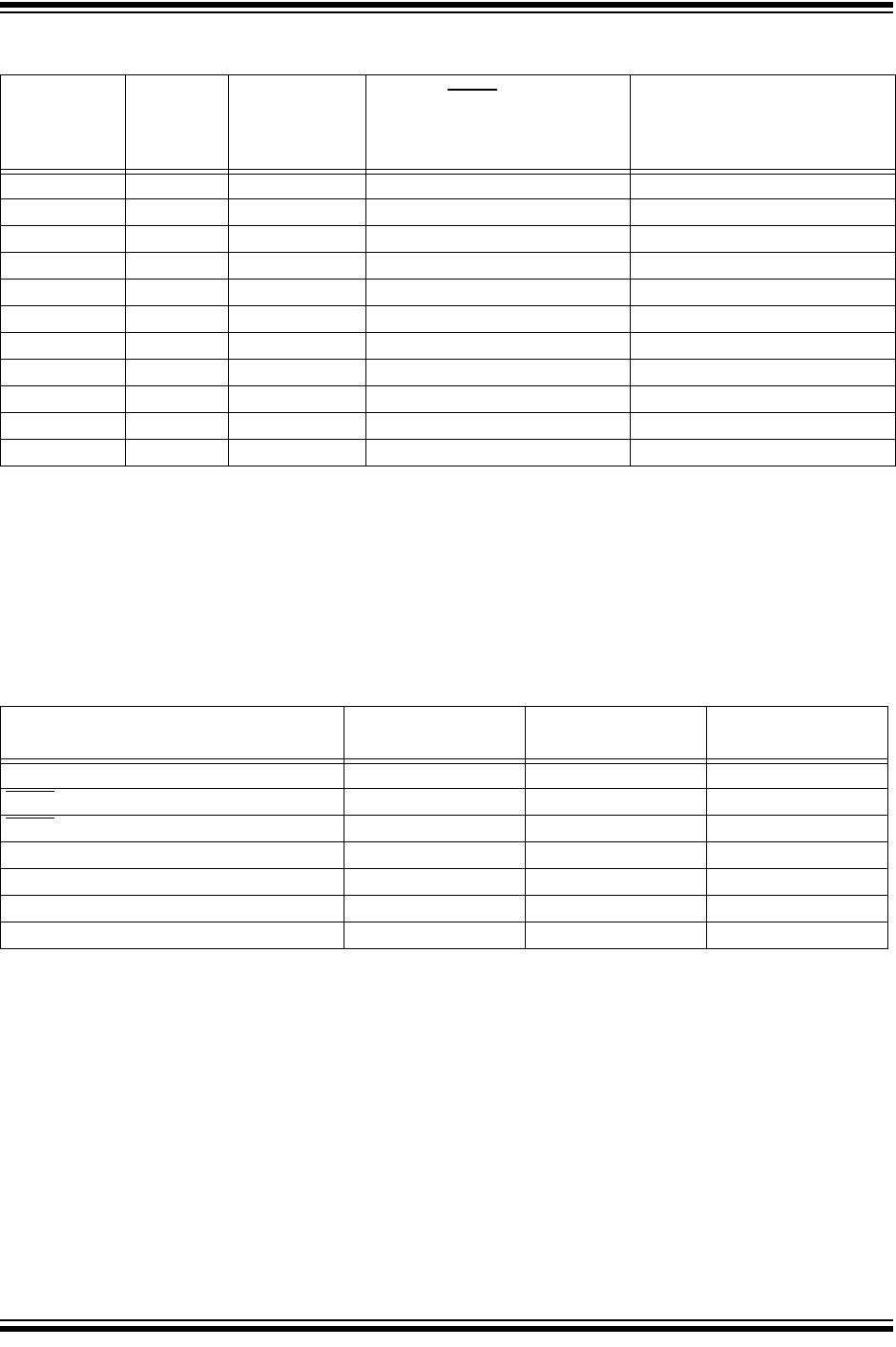
TABLE 14-5: INITIALIZATION CONDITION FOR SPECIAL REGISTERS
CM2CON1 109h 0000 0--0 0000 0--0 uuuu u--u
EEDAT 10Ch 0000 0000 0000 0000 uuuu uuuu
EEADR 10Dh 0000 0000 0000 0000 uuuu uuuu
EEDATH 10Eh --00 0000 --00 0000 --uu uuuu
EEADRH 10Fh ---0 0000 ---0 0000 ---u uuuu
SRCON 185h 0000 00-0 0000 00-0 uuuu uu-u
BAUDCTL 187h 01-0 0-00 01-0 0-00 uu-u u-uu
ANSEL 188h 1111 1111 1111 1111 uuuu uuuu
ANSELH 189h 1111 1111 1111 1111 uuuu uuuu
EECON1 18Ch ---- x000 ---- q000 ---- uuuu
EECON2 18Dh ---- ---- ---- ---- ---- ----
Condition
Program
Counter
Status
Register
PCON
Register
Power-on Reset 000h 0001 1xxx --01 --0x
MCLR
Reset during normal operation 000h 000u uuuu --0u --uu
MCLR Reset during Sleep 000h 0001 0uuu --0u --uu
WDT Reset 000h 0000 uuuu --0u --uu
WDT Wake-up PC + 1 uuu0 0uuu --uu --uu
Brown-out Reset 000h 0001 1uuu --01 --u0
Interrupt Wake-up from Sleep PC + 1
(1)
uuu1 0uuu --uu --uu
Legend: u = unchanged, x = unknown, — = unimplemented bit, reads as ‘0’.
Note 1: When the wake-up is due to an interrupt and Global Interrupt Enable bit, GIE, is set, the PC is loaded with
the interrupt vector (0004h) after execution of PC + 1.
TABLE 14-4: INITIALIZATION CONDITION FOR REGISTER (CONTINUED)
Register Address
Power-on
Reset
MCLR
Reset
WDT Reset (Continued)
Brown-out Reset
(1)
Wake-up from Sleep through
Interrupt
Wake-up from Sleep through
WDT Time-out (Continued)
Legend: u = unchanged, x = unknown, – = unimplemented bit, reads as ‘0’, q = value depends on condition.
Note 1: If VDD goes too low, Power-on Reset will be activated and registers will be affected differently.
2: One or more bits in INTCON and/or PIR1 will be affected (to cause wake-up).
3: When the wake-up is due to an interrupt and the GIE bit is set, the PC is loaded with the interrupt
vector (0004h).
4: See Table 14-5 for Reset value for specific condition.
5: If Reset was due to brown-out, then bit 0 = 0. All other Resets will cause bit 0 = u.
6: Accessible only when SSPCON register bits SSPM<3:0> = 1001.