
Datasheet


2006-2012 Microchip Technology Inc. DS41291G-page 193
PIC16F882/883/884/886/887
13.4 MSSP I
2
C Operation
The MSSP module in I
2
C mode, fully implements all
master and slave functions (including general call
support) and provides interrupts on Start and Stop bits in
hardware, to determine a free bus (Multi-Master mode).
The MSSP module implements the standard mode
specifications, as well as 7-bit and 10-bit addressing.
Two pins are used for data transfer. These are the
RC3/SCK/SCL pin, which is the clock (SCL), and the
RC4/SDI/SDA pin, which is the data (SDA). The user
must configure these pins as inputs or outputs through
the TRISC<4:3> bits.
The MSSP module functions are enabled by setting
MSSP Enable bit SSPEN of the SSPCON register.
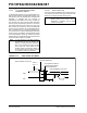
FIGURE 13-6: MSSP BLOCK DIAGRAM
(I
2
C MODE)
The MSSP module has these six registers for I
2
C
operation:
• MSSP Control Register 1 (SSPCON)
• MSSP Control Register 2 (SSPCON2)
• MSSP STATUS register (SSPSTAT)
• Serial Receive/Transmit Buffer (SSPBUF)
• MSSP Shift Register (SSPSR) – Not directly
accessible
• MSSP Address register (SSPADD)
• MSSP Mask register (SSPMSK)
The SSPCON register allows control of the I
2
C
operation. The SSPM<3:0> mode selection bits
(SSPCON register) allow one of the following I
2
C modes
to be selected:
•I
2
C Master mode, clock = OSC/4 (SSPADD +1)
•I
2
C Slave mode (7-bit address)
•I
2
C Slave mode (10-bit address)
•I
2
C Slave mode (7-bit address), with Start and
Stop bit interrupts enabled
•I
2
C Slave mode (10-bit address), with Start and
Stop bit interrupts enabled
•I
2
C firmware controlled master operation, slave is
idle
Selection of any I
2
C mode with the SSPEN bit set,
forces the SCL and SDA pins to be open drain,
provided these pins are programmed to be inputs by
setting the appropriate TRISC bits.
13.4.1 SLAVE MODE
In Slave mode, the SCL and SDA pins must be
configured as inputs (TRISC<4:3> set). The MSSP
module will override the input state with the output data
when required (slave-transmitter).
When an address is matched, or the data transfer after
an address match is received, the hardware
automatically will generate the Acknowledge (ACK
)
pulse and load the SSPBUF register with the received
value currently in the SSPSR register.
If either or both of the following conditions are true, the
MSSP module will not give this ACK
pulse:
a) The buffer full bit BF (SSPCON register) was set
before the transfer was received.
b) The overflow bit SSPOV (SSPCON register)
was set before the transfer was received.
In this event, the SSPSR register value is not loaded
into the SSPBUF, but bit SSPIF of the PIR1 register is
set. The BF bit is cleared by reading the SSPBUF
register, while bit SSPOV is cleared through software.
The SCL clock input must have a minimum high and
low for proper operation. The high and low times of the
I
2
C specification, as well as the requirement of the
MSSP module, are shown in timing parameter #100
and parameter #101.
Read Write
SSPSR Reg
Match Detect
SSPADD Reg
Start and
Stop bit Detect
SSPBUF Reg
Internal
Data Bus
Addr Match
Set, Reset
S, P bits
(SSPSTAT Reg)
RC3/SCK/SCL
RC4/
Shift
Clock
MSb
SDI/
LSb
SDA
Note: I/O pins have diode protection to V
DD and VSS.
SSPMSK Reg