
Datasheet


2001-2013 Microchip Technology Inc. DS39582C-page 195
PIC16F87XA
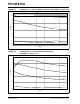
FIGURE 17-19: A/D CONVERSION TIMING
TABLE 17-15: A/D CONVERSION REQUIREMENTS
131
130
132
BSF ADCON0, GO
Q4
A/D CLK
A/D DATA
ADRES
ADIF
GO
SAMPLE
OLD_DATA
Sampling Stopped
DONE
NEW_DATA
(T
OSC/2)
(1)
987 210
Note: If the A/D clock source is selected as RC, a time of T
CY is added before the A/D clock starts. This allows the SLEEP
instruction to be executed.
1 TCY
Param
No.
Symbol Characteristic Min Typ† Max Units Conditions
130 T
AD A/D Clock Period PIC16F87XA 1.6 — — sTOSC based, VREF 3.0V
PIC16LF87XA 3.0 — — sT
OSC based, VREF 2.0V
PIC16F87XA 2.0 4.0 6.0 s A/D RC mode
PIC16LF87XA 3.0 6.0 9.0 s A/D RC mode
131 T
CNV Conversion Time (not including S/H time)
(Note 1)
—12TAD
132 TACQ Acquisition Time (Note 2)
10*
40
—
—
—
s
s The minimum time is the
amplifier settling time. This may
be used if the “new” input volt-
age has not changed by more
than 1 LSb (i.e., 20.0 mV @
5.12V) from the last sampled
voltage (as stated on C
HOLD).
134 T
GO Q4 to A/D Clock Start — TOSC/2 § — — If the A/D clock source is
selected as RC, a time of T
CY is
added before the A/D clock
starts. This allows the SLEEP
instruction to be executed.
* These parameters are characterized but not tested.
† Data in “Typ” column is at 5V, 25°C unless otherwise stated. These parameters are for design guidance only and are
not tested.
§ This specification ensured by design.
Note 1: ADRES register may be read on the following T
CY cycle.
2: See Section 11.1 “A/D Acquisition Requirements” for minimum conditions.