
Datasheet


PIC16F87X
DS30292C-page 104 2001 Microchip Technology Inc.
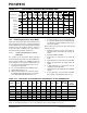
FIGURE 10-7: ASYNCHRONOUS RECEPTION WITH ADDRESS DETECT
FIGURE 10-8: ASYNCHRONOUS RECEPTION WITH ADDRESS BYTE FIRST
TABLE 10-7: REGISTERS ASSOCIATED WITH ASYNCHRONOUS RECEPTION
START
bit
bit1bit0
bit8 bit0STOP
bit
START
bit bit8
STOP
bit
RC7/RX/DT (pin)
Load RSR
Read
RCIF
Word 1
RCREG
Bit8 = 0, Data Byte Bit8 = 1, Address Byte
Note: This timing diagram shows a data byte followed by an address byte. The data byte is not read into the RCREG (receive buffer)
because ADDEN = 1.
START
bit
bit1bit0
bit8 bit0STOP
bit
START
bit bit8
STOP
bit
RC7/RX/DT (pin)
Load RSR
Read
RCIF
Word 1
RCREG
Bit8 = 1, Address Byte Bit8 = 0, Data Byte
Note: This timing diagram shows a data byte followed by an address byte. The data byte is not read into the RCREG (receive buffer)
because ADDEN was not updated and still = 0.
Address Name Bit 7 Bit 6 Bit 5 Bit 4 Bit 3 Bit 2 Bit 1 Bit 0
Value on:
POR,
BOR
Value on
all other
RESETS
0Bh, 8Bh,
10Bh,18Bh
INTCON GIE PEIE
T0IE INTE RBIE T0IF INTF R0IF 0000 000x 0000 000u
0Ch PIR1 PSPIF
(1)
ADIF RCIF TXIF SSPIF CCP1IF TMR2IF TMR1IF 0000 0000 0000 0000
18h RCSTA SPEN RX9 SREN CREN ADDEN FERR OERR RX9D 0000 000x 0000 000x
1Ah RCREG USART Receive Register 0000 0000 0000 0000
8Ch PIE1 PSPIE
(1)
ADIE RCIE TXIE SSPIE CCP1IE TMR2IE TMR1IE 0000 0000 0000 0000
98h TXSTA CSRC TX9 TXEN SYNC — BRGH TRMT TX9D 0000 -010 0000 -010
99h SPBRG Baud Rate Generator Register 0000 0000 0000 0000
Legend: x = unknown, - = unimplemented locations read as '0'. Shaded cells are not used for asynchronous reception.
Note 1: Bits PSPIE and PSPIF are reserved on PIC16F873/876 devices; always maintain these bits clear.