
Datasheet


2001-2013 Microchip Technology Inc. DS35007C-page 7
PIC16F84A
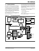
2.3 Special Function Registers
The Special Function Registers (Figure 2-2 and
Table 2-1) are used by the CPU and Peripheral
functions to control the device operation. These
registers are static RAM.
The special function registers can be classified into two
sets, core and peripheral. Those associated with the
core functions are described in this section. Those
related to the operation of the peripheral features are
described in the section for that specific feature.
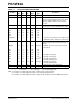
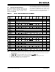
TABLE 2-1: SPECIAL FUNCTION REGISTER FILE SUMMARY
Addr Name Bit 7 Bit 6 Bit 5 Bit 4 Bit 3 Bit 2 Bit 1 Bit 0
Value on
Power-on
RESET
Details
on page
Bank 0
00h INDF Uses contents of FSR to address Data Memory (not a physical register) ---- ---- 11
01h TMR0 8-bit Real-Time Clock/Counter xxxx xxxx 20
02h PCL Low Order 8 bits of the Program Counter (PC) 0000 0000 11
03h
STATUS
(2)
IRP RP1 RP0 TO PD ZDCC
0001 1xxx
8
04h FSR Indirect Data Memory Address Pointer 0 xxxx xxxx 11
05h PORTA
(4)
— — — RA4/T0CKI RA3 RA2 RA1 RA0 ---x xxxx 16
06h PORTB
(5)
RB7 RB6 RB5 RB4 RB3 RB2 RB1 RB0/INT xxxx xxxx 18
07h — Unimplemented location, read as '0' — —
08h EEDATA EEPROM Data Register xxxx xxxx 13,14
09h EEADR EEPROM Address Register xxxx xxxx 13,14
0Ah
PCLATH
— — — Write Buffer for upper 5 bits of the PC
(1)
---0 0000
11
0Bh INTCON GIE EEIE T0IE INTE RBIE T0IF INTF RBIF 0000 000x 10
Bank 1
80h INDF Uses Contents of FSR to address Data Memory (not a physical register) ---- ---- 11
81h
OPTION_REG RBPU INTEDG T0CS T0SE PSA PS2 PS1 PS0
1111 1111
9
82h PCL Low order 8 bits of Program Counter (PC) 0000 0000 11
83h
STATUS
(2)
IRP RP1 RP0 TO PD ZDCC
0001 1xxx
8
84h FSR Indirect data memory address pointer 0 xxxx xxxx 11
85h TRISA
— — — PORTA Data Direction Register ---1 1111 16
86h TRISB PORTB Data Direction Register 1111 1111 18
87h — Unimplemented location, read as '0' — —
88h EECON1
— — — EEIF WRERR WREN WR RD ---0 x000 13
89h
EECON2 EEPROM Control Register 2 (not a physical register)
---- ----
14
0Ah
PCLATH
— — — Write buffer for upper 5 bits of the PC
(1)
---0 0000
11
0Bh INTCON GIE EEIE T0IE INTE RBIE T0IF INTF RBIF 0000 000x 10
Legend: x = unknown, u = unchanged. - = unimplemented, read as '0', q = value depends on condition
Note 1: The upper byte of the program counter is not directly accessible. PCLATH is a slave register for PC<12:8>. The contents
of PCLATH can be transferred to the upper byte of the program counter, but the contents of PC<12:8> are never trans-
ferred to PCLATH.
2: The TO
and PD status bits in the STATUS register are not affected by a MCLR Reset.
3: Other (non power-up) RESETS include: external RESET through MCLR
and the Watchdog Timer Reset.
4: On any device RESET, these pins are configured as inputs.
5: This is the value that will be in the port output latch.