
Datasheet


2001-2013 Microchip Technology Inc. DS35007C-page 51
PIC16F84A
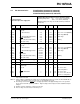
9.2 DC Characteristics: PIC16F84A-04 (Commercial, Industrial)
PIC16F84A-20 (Commercial, Industrial)
PIC16LF84A-04 (Commercial, Industrial)
DC Characteristics
All Pins Except Power Supply Pins
Standard Operating Conditions (unless otherwise stated)
Operating temperature 0C T
A +70C (commercial)
-40C T
A +85C (industrial)
Operating voltage V
DD range as described in DC specifications
(Section 9.1)
Param
No.
Symbol Characteristic Min Typ† Max Units Conditions
V
IL Input Low Voltage
I/O ports:
D030 with TTL buffer V
SS —0.8 V4.5V VDD 5.5V (Note 4)
D030A VSS —0.16VDD V Entire range (Note 4)
D031 with Schmitt Trigger buffer V
SS —0.2VDD V Entire range
D032 MCLR, RA4/T0CKI VSS —0.2VDD V
D033 OSC1 (XT, HS and LP modes) VSS —0.3VDD V (Note 1)
D034 OSC1 (RC mode) V
SS —0.1VDD V
VIH Input High Voltage
I/O ports: —
D040
D040A
with TTL buffer 2.0
0.25V
DD+0.8
—
—
V
DD
VDD
V
V
4.5V VDD 5.5V (Note 4)
Entire range (Note 4)
D041 with Schmitt Trigger buffer 0.8 V
DD —VDD Entire range
D042 MCLR
, 0.8 VDD —VDD V
D042A RA4/T0CKI 0.8 VDD —8.5 V
D043 OSC1 (XT, HS and LP modes) 0.8 VDD —VDD V (Note 1)
D043A OSC1 (RC mode) 0.9 V
DD VDD V
D050 VHYS Hysteresis of Schmitt Trigger
Inputs
—0.1—V
D070 I
PURB PORTB Weak Pull-up Current 50 250 400 AVDD = 5.0V, VPIN = VSS
IIL Input Leakage Current
(Notes 2, 3)
D060 I/O ports — — 1 AVss V
PIN VDD,
Pin at hi-impedance
D061 MCLR
, RA4/T0CKI — — 5 AVss VPIN VDD
D063 OSC1 — — 5 AVss VPIN VDD, XT, HS
and LP osc configuration
† Data in “Typ” column is at 5.0V, 25C unless otherwise stated. These parameters are for design guidance
only and are not tested.
Note 1: In RC oscillator configuration, the OSC1 pin is a Schmitt Trigger input. Do not drive the PIC16F84A with an
external clock while the device is in RC mode, or chip damage may result.
2: The leakage current on the MCLR
pin is strongly dependent on the applied voltage level. The specified
levels represent normal operating conditions. Higher leakage current may be measured at different input
voltages.
3: Negative current is defined as coming out of the pin.
4: The user may choose the better of the two specs.