
Datasheet


2001-2013 Microchip Technology Inc. DS35007C-page 3
PIC16F84A
1.0 DEVICE OVERVIEW
This document contains device specific information for
the operation of the PIC16F84A device. Additional
information may be found in the PIC
®
Mid-Range Ref-
erence Manual, (DS33023), which may be downloaded
from the Microchip website. The Reference Manual
should be considered a complementary document to
this data sheet, and is highly recommended reading for
a better understanding of the device architecture and
operation of the peripheral modules.
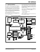
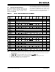
The PIC16F84A belongs to the mid-range family of the
PIC
®
microcontroller devices. A block diagram of the
device is shown in Figure 1-1.
The program memory contains 1K words, which trans-
lates to 1024 instructions, since each 14-bit program
memory word is the same width as each device instruc-
tion. The data memory (RAM) contains 68 bytes. Data
EEPROM is 64 bytes.
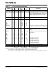
There are also 13 I/O pins that are user-configured on
a pin-to-pin basis. Some pins are multiplexed with other
device functions. These functions include:
• External interrupt
• Change on PORTB interrupt
• Timer0 clock input
Table 1-1 details the pinout of the device with descrip-
tions and details for each pin.
FIGURE 1-1: PIC16F84A BLOCK DIAGRAM
FLASH
Program
Memory
Program Counter
13
Program
Bus
Instruction Register
8 Level Stack
(13-bit)
Direct Addr
8
Instruction
Decode &
Control
Timing
Generation
OSC2/CLKOUT
OSC1/CLKIN
Power-up
Timer
Oscillator
Start-up Timer
Power-on
Reset
Watchdog
Timer
MCLR
VDD, VSS
W reg
ALU
MUX
I/O Ports
TMR0
STATUS reg
FSR reg
Indirect
Addr
RA3:RA0
RB7:RB1
RA4/T0CKI
EEADR
EEPROM
Data Memory
64 x 8
EEDATA
Addr Mux
RAM Addr
RAM
File Registers
EEPROM Data Memory
Data Bus
5
7
7
RB0/INT
14
8
8
1K x 14
68 x 8