
Datasheet


2001-2013 Microchip Technology Inc. DS35007C-page 15
PIC16F84A
4.0 I/O PORTS
Some pins for these I/O ports are multiplexed with an
alternate function for the peripheral features on the
device. In general, when a peripheral is enabled, that
pin may not be used as a general purpose I/O pin.
Additional information on I/O ports may be found in the
PIC
®
Mid-Range Reference Manual (DS33023).
4.1 PORTA and TRISA Registers
PORTA is a 5-bit wide, bi-directional port. The corre-
sponding data direction register is TRISA. Setting a
TRISA bit (= 1) will make the corresponding PORTA pin
an input (i.e., put the corresponding output driver in a
Hi-Impedance mode). Clearing a TRISA bit (= 0) will
make the corresponding PORTA pin an output (i.e., put
the contents of the output latch on the selected pin).
Reading the PORTA register reads the status of the
pins, whereas writing to it will write to the port latch. All
write operations are read-modify-write operations.
Therefore, a write to a port implies that the port pins are
read. This value is modified and then written to the port
data latch.
Pin RA4 is multiplexed with the Timer0 module clock
input to become the RA4/T0CKI pin. The RA4/T0CKI
pin is a Schmitt Trigger input and an open drain output.
All other RA port pins have TTL input levels and full
CMOS output drivers.
EXAMPLE 4-1: INITIALIZING PORTA
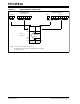
FIGURE 4-1: BLOCK DIAGRAM OF
PINS RA3:RA0
FIGURE 4-2: BLOCK DIAGRAM OF PIN
RA4
Note: On a Power-on Reset, these pins are con-
figured as inputs and read as '0'.
BCF STATUS, RP0 ;
CLRF PORTA ; Initialize PORTA by
; clearing output
; data latches
BSF STATUS, RP0 ; Select Bank 1
MOVLW 0x0F ; Value used to
; initialize data
; direction
MOVWF TRISA ; Set RA<3:0> as inputs
; RA4 as output
; TRISA<7:5> are always
; read as '0'.
Data
Bus
Q
D
Q
CK
QD
Q
CK
QD
EN
P
N
WR
Port
WR
TRIS
Data Latch
TRIS Latch
RD TRIS
RD Port
TTL
Input
Buffer
V
SS
VDD
I/O pin
Note: I/O pins have protection diodes to VDD and VSS.
Data
Bus
WR
Port
WR
TRIS
RD Port
Data Latch
TRIS Latch
RD TRIS
Schmitt
Trigger
Input
Buffer
N
V
SS
RA4 pin
TMR0 Clock Input
QD
Q
CK
QD
Q
CK
EN
QD
EN
Note: I/O pins have protection diodes to VDD and VSS.