PIC16F84A 18-pin Enhanced FLASH/EEPROM 8-Bit Microcontroller High Performance RISC CPU Features: • 13 I/O pins with individual direction control • High current sink/source for direct LED drive - 25 mA sink max. per pin - 25 mA source max.
PIC16F84A Table of Contents 1.0 Device Overview .......................................................................................................................................................................... 3 2.0 Memory Organization ................................................................................................................................................................... 5 3.0 Data EEPROM Memory ..............................................................................
PIC16F84A 1.0 DEVICE OVERVIEW The program memory contains 1K words, which translates to 1024 instructions, since each 14-bit program memory word is the same width as each device instruction. The data memory (RAM) contains 68 bytes. Data EEPROM is 64 bytes. This document contains device specific information for the operation of the PIC16F84A device. Additional information may be found in the PIC® Mid-Range Reference Manual, (DS33023), which may be downloaded from the Microchip website.
PIC16F84A TABLE 1-1: PIC16F84A PINOUT DESCRIPTION PDIP No. SOIC No. SSOP No. I/O/P Type OSC1/CLKIN 16 16 18 I OSC2/CLKOUT 15 15 19 O — Oscillator crystal output. Connects to crystal or resonator in Crystal Oscillator mode. In RC mode, OSC2 pin outputs CLKOUT, which has 1/4 the frequency of OSC1 and denotes the instruction cycle rate. MCLR 4 4 4 I/P ST Master Clear (Reset) input/programming voltage input. This pin is an active low RESET to the device.
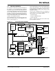
PIC16F84A MEMORY ORGANIZATION There are two memory blocks in the PIC16F84A. These are the program memory and the data memory. Each block has its own bus, so that access to each block can occur during the same oscillator cycle. The data memory can further be broken down into the general purpose RAM and the Special Function Registers (SFRs). The operation of the SFRs that control the “core” are described here.
PIC16F84A 2.2 Data Memory Organization The data memory is partitioned into two areas. The first is the Special Function Registers (SFR) area, while the second is the General Purpose Registers (GPR) area. The SFRs control the operation of the device. Portions of data memory are banked. This is for both the SFR area and the GPR area. The GPR area is banked to allow greater than 116 bytes of general purpose RAM. The banked areas of the SFR are for the registers that control the peripheral functions.
PIC16F84A 2.3 Special Function Registers The special function registers can be classified into two sets, core and peripheral. Those associated with the core functions are described in this section. Those related to the operation of the peripheral features are described in the section for that specific feature. The Special Function Registers (Figure 2-2 and Table 2-1) are used by the CPU and Peripheral functions to control the device operation. These registers are static RAM.
PIC16F84A 2.3.1 STATUS REGISTER Note 1: The IRP and RP1 bits (STATUS<7:6>) are not used by the PIC16F84A and should be programmed as cleared. Use of these bits as general purpose R/W bits is NOT recommended, since this may affect upward compatibility with future products. The STATUS register contains the arithmetic status of the ALU, the RESET status and the bank select bit for data memory. As with any register, the STATUS register can be the destination for any instruction.
PIC16F84A 2.3.2 OPTION REGISTER Note: The OPTION register is a readable and writable register which contains various control bits to configure the TMR0/WDT prescaler, the external INT interrupt, TMR0, and the weak pull-ups on PORTB. REGISTER 2-2: When the prescaler is assigned to the WDT (PSA = '1'), TMR0 has a 1:1 prescaler assignment.
PIC16F84A 2.3.3 INTCON REGISTER Note: The INTCON register is a readable and writable register that contains the various enable bits for all interrupt sources. REGISTER 2-3: Interrupt flag bits are set when an interrupt condition occurs, regardless of the state of its corresponding enable bit or the global enable bit, GIE (INTCON<7>).
PIC16F84A 2.4 PCL and PCLATH The program counter (PC) specifies the address of the instruction to fetch for execution. The PC is 13 bits wide. The low byte is called the PCL register. This register is readable and writable. The high byte is called the PCH register. This register contains the PC<12:8> bits and is not directly readable or writable. If the program counter (PC) is modified or a conditional test is true, the instruction requires two cycles. The second cycle is executed as a NOP.
PIC16F84A FIGURE 2-3: DIRECT/INDIRECT ADDRESSING Indirect Addressing Direct Addressing RP1 RP0 6 From Opcode 0 IRP (2) 7 (FSR) 0 (2) Bank Select Location Select Bank Select 00 Location Select 01 00h 80h 0Bh 0Ch Addresses map back to Bank 0 Data Memory(1) 4Fh 50h 7Fh (3) (3) Bank 0 Bank 1 FFh Note 1: For memory map detail, see Figure 2-2. 2: Maintain as clear for upward compatibility with future products. 3: Not implemented. DS35007C-page 12 2001-2013 Microchip Technology Inc.
PIC16F84A 3.0 DATA EEPROM MEMORY The EEPROM data memory is readable and writable during normal operation (full VDD range). This memory is not directly mapped in the register file space. Instead it is indirectly addressed through the Special Function Registers. There are four SFRs used to read and write this memory. These registers are: The EEPROM data memory allows byte read and write. A byte write automatically erases the location and writes the new data (erase before write).
PIC16F84A 3.1 Reading the EEPROM Data Memory Additionally, the WREN bit in EECON1 must be set to enable write. This mechanism prevents accidental writes to data EEPROM due to errant (unexpected) code execution (i.e., lost programs). The user should keep the WREN bit clear at all times, except when updating EEPROM. The WREN bit is not cleared by hardware. To read a data memory location, the user must write the address to the EEADR register and then set control bit RD (EECON1<0>).
PIC16F84A 4.0 I/O PORTS FIGURE 4-1: Some pins for these I/O ports are multiplexed with an alternate function for the peripheral features on the device. In general, when a peripheral is enabled, that pin may not be used as a general purpose I/O pin. Additional information on I/O ports may be found in the PIC® Mid-Range Reference Manual (DS33023). 4.1 Data Bus BLOCK DIAGRAM OF PINS RA3:RA0 D Q VDD WR Port Q CK P Data Latch PORTA and TRISA Registers N PORTA is a 5-bit wide, bi-directional port.
PIC16F84A TABLE 4-1: PORTA FUNCTIONS Name Bit0 Buffer Type RA0 RA1 RA2 RA3 RA4/T0CKI bit0 bit1 bit2 bit3 bit4 TTL TTL TTL TTL ST Function Input/output Input/output Input/output Input/output Input/output or external clock input for TMR0. Output is open drain type.
PIC16F84A 4.2 PORTB and TRISB Registers PORTB is an 8-bit wide, bi-directional port. The corresponding data direction register is TRISB. Setting a TRISB bit (= 1) will make the corresponding PORTB pin an input (i.e., put the corresponding output driver in a Hi-Impedance mode). Clearing a TRISB bit (= 0) will make the corresponding PORTB pin an output (i.e., put the contents of the output latch on the selected pin).
PIC16F84A TABLE 4-3: PORTB FUNCTIONS Name RB0/INT Bit Buffer Type bit0 TTL/ST(1) I/O Consistency Function Input/output pin or external interrupt input. Internal software programmable weak pull-up. RB1 bit1 TTL Input/output pin. Internal software programmable weak pull-up. RB2 bit2 TTL Input/output pin. Internal software programmable weak pull-up. RB3 bit3 TTL Input/output pin. Internal software programmable weak pull-up. RB4 bit4 TTL Input/output pin (with interrupt-on-change).
PIC16F84A 5.0 TIMER0 MODULE Additional information on external clock requirements is available in the PIC® Mid-Range Reference Manual, (DS33023). The Timer0 module timer/counter has the following features: • • • • • • 5.
PIC16F84A 5.2.1 SWITCHING PRESCALER ASSIGNMENT 5.3 The TMR0 interrupt is generated when the TMR0 register overflows from FFh to 00h. This overflow sets bit T0IF (INTCON<2>). The interrupt can be masked by clearing bit T0IE (INTCON<5>). Bit T0IF must be cleared in software by the Timer0 module Interrupt Service Routine before re-enabling this interrupt. The TMR0 interrupt cannot awaken the processor from SLEEP since the timer is shut-off during SLEEP.
PIC16F84A 6.0 SPECIAL FEATURES OF THE CPU the chip in RESET until the crystal oscillator is stable. The other is the Power-up Timer (PWRT), which provides a fixed delay of 72 ms (nominal) on power-up only. This design keeps the device in RESET while the power supply stabilizes. With these two timers on-chip, most applications need no external RESET circuitry. What sets a microcontroller apart from other processors are special circuits to deal with the needs of real time applications.
PIC16F84A 6.2 Oscillator Configurations 6.2.1 FIGURE 6-2: OSCILLATOR TYPES The PIC16F84A can be operated in four different oscillator modes. The user can program two configuration bits (FOSC1 and FOSC0) to select one of these four modes: • • • • LP XT HS RC 6.2.
PIC16F84A TABLE 6-2: Mode LP XT HS Note: CAPACITOR SELECTION FOR CRYSTAL OSCILLATOR Freq OSC1/C1 OSC2/C2 32 kHz 68 - 100 pF 68 - 100 pF 200 kHz 15 - 33 pF 15 - 33 pF 100 kHz 100 - 150 pF 100 - 150 pF 2 MHz 15 - 33 pF 15 - 33 pF 4 MHz 15 - 33 pF 15 - 33 pF 4 MHz 15 - 33 pF 15 - 33 pF 20 MHz 15 - 33 pF 15 - 33 pF Higher capacitance increases the stability of the oscillator, but also increases the start-up time. These values are for design guidance only.
PIC16F84A 6.3 RESET The PIC16F84A differentiates between various kinds of RESET: • • • • • Power-on Reset (POR) MCLR during normal operation MCLR during SLEEP WDT Reset (during normal operation) WDT Wake-up (during SLEEP) Figure 6-4 shows a simplified block diagram of the On-Chip RESET Circuit. The MCLR Reset path has a noise filter to ignore small pulses. The electrical specifications state the pulse width requirements for the MCLR pin.
PIC16F84A TABLE 6-4: Register RESET CONDITIONS FOR ALL REGISTERS MCLR during: – normal operation – SLEEP WDT Reset during normal operation Wake-up from SLEEP: – through interrupt – through WDT Time-out Address Power-on Reset — xxxx xxxx uuuu uuuu uuuu uuuu INDF 00h ---- ---- ---- ---- ---- ---- TMR0 01h xxxx xxxx uuuu uuuu uuuu uuuu PCL 02h 0000 0000 0000 0000 STATUS 03h 0001 1xxx 000q quuu(3) uuuq quuu(3) FSR 04h xxxx xxxx uuuu uuuu uuuu uuuu PORTA(4) 05h ---x xxxx ---u
PIC16F84A 6.4 Power-on Reset (POR) A Power-on Reset pulse is generated on-chip when VDD rise is detected (in the range of 1.2V - 1.7V). To take advantage of the POR, just tie the MCLR pin directly (or through a resistor) to VDD. This will eliminate external RC components usually needed to create Power-on Reset. A minimum rise time for VDD must be met for this to operate properly. See Electrical Specifications for details. 6.
PIC16F84A FIGURE 6-6: TIME-OUT SEQUENCE ON POWER-UP (MCLR NOT TIED TO VDD): CASE 1 VDD MCLR INTERNAL POR TPWRT PWRT TIME-OUT TOST OST TIME-OUT INTERNAL RESET TIME-OUT SEQUENCE ON POWER-UP (MCLR NOT TIED TO VDD): CASE 2 FIGURE 6-7: VDD MCLR INTERNAL POR TPWRT PWRT TIME-OUT TOST OST TIME-OUT INTERNAL RESET FIGURE 6-8: TIME-OUT SEQUENCE ON POWER-UP (MCLR TIED TO VDD): FAST VDD RISE TIME VDD MCLR INTERNAL POR TPWRT PWRT TIME-OUT TOST OST TIME-OUT INTERNAL RESET 2001-2013 Microchip Technology
PIC16F84A FIGURE 6-9: TIME-OUT SEQUENCE ON POWER-UP (MCLR TIED TO VDD): SLOW VDD RISE TIME V1 VDD MCLR INTERNAL POR TPWRT PWRT TIME-OUT TOST OST TIME-OUT INTERNAL RESET When VDD rises very slowly, it is possible that the TPWRT time-out and TOST time-out will expire before VDD has reached its final value. In this example, the chip will reset properly if, and only if, V1 VDD min. 6.
PIC16F84A 6.8 6.8.1 Interrupts The PIC16F84A has 4 sources of interrupt: • • • • External interrupt RB0/INT pin TMR0 overflow interrupt PORTB change interrupts (pins RB7:RB4) Data EEPROM write complete interrupt The interrupt control register (INTCON) records individual interrupt requests in flag bits. It also contains the individual and global interrupt enable bits. The global interrupt enable bit, GIE (INTCON<7>), enables (if set) all unmasked interrupts or disables (if cleared) all interrupts.
PIC16F84A 6.9 Context Saving During Interrupts During an interrupt, only the return PC value is saved on the stack. Typically, users wish to save key register values during an interrupt (e.g., W register and STATUS register). This is implemented in software. The code in Example 6-1 stores and restores the STATUS and W register’s values. The user defined registers, W_TEMP and STATUS_TEMP are the temporary storage locations for the W and STATUS registers values. EXAMPLE 6-1: PUSH ISR POP 6.
PIC16F84A 6.10.2 WDT PROGRAMMING CONSIDERATIONS It should also be taken into account that under worst case conditions (VDD = Min., Temperature = Max., Max. WDT Prescaler), it may take several seconds before a WDT time-out occurs. FIGURE 6-11: WATCHDOG TIMER BLOCK DIAGRAM From TMR0 Clock Source (Figure 5-2) 0 WDT Timer 1 • M Postscaler U 8 X PS2:PS0 8 - to -1 MUX PSA WDT Enable Bit • To TMR0 (Figure 5-2) 1 0 MUX PSA WDT Time-out Note: PSA and PS2:PS0 are bits in the OPTION_REG register.
PIC16F84A 6.11 6.11.2 Power-down Mode (SLEEP) A device may be powered down (SLEEP) and later powered up (wake-up from SLEEP). 6.11.1 SLEEP The Power-down mode is entered by executing the SLEEP instruction. If enabled, the Watchdog Timer is cleared (but keeps running), the PD bit (STATUS<3>) is cleared, the TO bit (STATUS<4>) is set, and the oscillator driver is turned off. The I/O ports maintain the status they had before the SLEEP instruction was executed (driving high, low, or hi-impedance).
PIC16F84A 6.11.3 WAKE-UP USING INTERRUPTS When global interrupts are disabled (GIE cleared) and any interrupt source has both its interrupt enable bit and interrupt flag bit set, one of the following will occur: • If the interrupt occurs before the execution of a SLEEP instruction, the SLEEP instruction will complete as a NOP. Therefore, the WDT and WDT postscaler will not be cleared, the TO bit will not be set and PD bits will not be cleared.
PIC16F84A NOTES: DS35007C-page 34 2001-2013 Microchip Technology Inc.
PIC16F84A 7.0 INSTRUCTION SET SUMMARY Each PIC16CXX instruction is a 14-bit word, divided into an OPCODE which specifies the instruction type and one or more operands which further specify the operation of the instruction. The PIC16CXX instruction set summary in Table 7-2 lists byte-oriented, bit-oriented, and literal and control operations. Table 7-1 shows the opcode field descriptions. For byte-oriented instructions, 'f' represents a file register designator and 'd' represents a destination designator.
PIC16F84A TABLE 7-2: PIC16CXXX INSTRUCTION SET Mnemonic, Operands 14-Bit Opcode Description Cycles MSb LSb Status Affected Notes BYTE-ORIENTED FILE REGISTER OPERATIONS ADDWF ANDWF CLRF CLRW COMF DECF DECFSZ INCF INCFSZ IORWF MOVF MOVWF NOP RLF RRF SUBWF SWAPF XORWF f, d f, d f f, d f, d f, d f, d f, d f, d f, d f f, d f, d f, d f, d f, d Add W and f AND W with f Clear f Clear W Complement f Decrement f Decrement f, Skip if 0 Increment f Increment f, Skip if 0 Inclusive OR W with f Move f Move W to
PIC16F84A 7.1 Instruction Descriptions ADDLW Add Literal and W BCF Bit Clear f Syntax: [label] ADDLW Syntax: [label] BCF Operands: 0 f 127 0b7 k f,b Operands: 0 k 255 Operation: (W) + k (W) Status Affected: C, DC, Z Operation: 0 (f) Description: The contents of the W register are added to the eight-bit literal 'k' and the result is placed in the W register. Status Affected: None Description: Bit 'b' in register 'f' is cleared.
PIC16F84A BTFSC Bit Test, Skip if Clear CLRWDT Clear Watchdog Timer Syntax: [label] BTFSC f,b Syntax: [ label ] CLRWDT Operands: 0 f 127 0b7 Operands: None Operation: Operation: skip if (f) = 0 Status Affected: None Description: If bit 'b' in register 'f' is '1', the next instruction is executed. If bit 'b' in register 'f' is '0', the next instruction is discarded, and a NOP is executed instead, making this a 2TCY instruction.
PIC16F84A DECFSZ Decrement f, Skip if 0 INCFSZ Increment f, Skip if 0 Syntax: [ label ] DECFSZ f,d Syntax: [ label ] Operands: 0 f 127 d [0,1] Operands: 0 f 127 d [0,1] Operation: (f) - 1 (destination); skip if result = 0 Operation: (f) + 1 (destination), skip if result = 0 Status Affected: None Status Affected: None Description: The contents of register 'f' are decremented. If 'd' is 0, the result is placed in the W register.
PIC16F84A MOVF Move f Syntax: [ label ] Operands: 0 f 127 d [0,1] MOVF f,d RETFIE Return from Interrupt Syntax: [ label ] RETFIE Operands: None Operation: TOS PC, 1 GIE Status Affected: None Operation: (f) (destination) Status Affected: Z Description: The contents of register f are moved to a destination dependant upon the status of d. If d = 0, destination is W register. If d = 1, the destination is file register f itself.
PIC16F84A RLF Rotate Left f through Carry SUBLW Subtract W from Literal Syntax: [ label ] RLF Syntax: [ label ] SUBLW k Operands: 0 f 127 d [0,1] Operands: 0 k 255 Operation: k - (W) W) Operation: See description below Status Affected: C, DC, Z Status Affected: C Description: Description: The contents of register 'f' are rotated one bit to the left through the Carry Flag. If 'd' is 0, the result is placed in the W register.
PIC16F84A XORLW Exclusive OR Literal with W XORWF Syntax: [label] Operands: 0 f 127 d [0,1] Syntax: [label] Operands: 0 k 255 Operation: (W) .XOR. k W) Status Affected: Z Operation: (W) .XOR. (f) destination) The contents of the W register are XOR’ed with the eight-bit literal 'k'. The result is placed in the W register. Status Affected: Z Description: Exclusive OR the contents of the W register with register 'f'. If 'd' is 0, the result is stored in the W register.
8.
8.2 MPLAB C Compilers for Various Device Families The MPLAB C Compiler code development systems are complete ANSI C compilers for Microchip’s PIC18, PIC24 and PIC32 families of microcontrollers and the dsPIC30 and dsPIC33 families of digital signal controllers. These compilers provide powerful integration capabilities, superior code optimization and ease of use. For easy source level debugging, the compilers provide symbol information that is optimized to the MPLAB IDE debugger. 8.
8.7 MPLAB SIM Software Simulator The MPLAB SIM Software Simulator allows code development in a PC-hosted environment by simulating the PIC MCUs and dsPIC® DSCs on an instruction level. On any given instruction, the data areas can be examined or modified and stimuli can be applied from a comprehensive stimulus controller. Registers can be logged to files for further run-time analysis.
8.11 PICkit 2 Development Programmer/Debugger and PICkit 2 Debug Express The PICkit™ 2 Development Programmer/Debugger is a low-cost development tool with an easy to use interface for programming and debugging Microchip’s Flash families of microcontrollers.
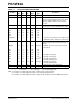
PIC16F84A 9.0 ELECTRICAL CHARACTERISTICS Absolute Maximum Ratings † Ambient temperature under bias.............................................................................................................-55C to +125C Storage temperature .............................................................................................................................. -65C to +150C Voltage on any pin with respect to VSS (except VDD, MCLR, and RA4) ......................................... -0.
PIC16F84A FIGURE 9-1: PIC16F84A-20 VOLTAGE-FREQUENCY GRAPH 6.0V 5.5V 5.0V Voltage 4.5V 4.0V 3.5V 3.0V 2.5V 2.0V 20 MHz Frequency FIGURE 9-2: PIC16LF84A-04 VOLTAGEFREQUENCY GRAPH FIGURE 9-3: PIC16F84A-04 VOLTAGEFREQUENCY GRAPH 5.5V 6.0V 5.0V 5.5V 4.5V 5.0V 4.0V 4.5V 3.5V 4.0V Voltage Voltage 6.0V 3.0V 2.5V 3.5V 3.0V 2.5V 2.0V 2.0V 4 MHz 10 MHz Frequency FMAX = (6.0 MHz/V) (VDDAPPMIN - 2.
PIC16F84A 9.
PIC16F84A 9.
PIC16F84A 9.2 DC Characteristics: PIC16F84A-04 (Commercial, Industrial) PIC16F84A-20 (Commercial, Industrial) PIC16LF84A-04 (Commercial, Industrial) DC Characteristics All Pins Except Power Supply Pins Param Symbol No. VIL Characteristic Standard Operating Conditions (unless otherwise stated) Operating temperature 0C TA +70C (commercial) -40C TA +85C (industrial) Operating voltage VDD range as described in DC specifications (Section 9.
PIC16F84A 9.2 DC Characteristics: PIC16F84A-04 (Commercial, Industrial) PIC16F84A-20 (Commercial, Industrial) PIC16LF84A-04 (Commercial, Industrial) (Continued) DC Characteristics All Pins Except Power Supply Pins Param Symbol No. VOL Characteristic Standard Operating Conditions (unless otherwise stated) Operating temperature 0C TA +70C (commercial) -40C TA +85C (industrial) Operating voltage VDD range as described in DC specifications (Section 9.
PIC16F84A 9.3 9.3.1 AC (Timing) Characteristics TIMING PARAMETER SYMBOLOGY The timing parameter symbols have been created following one of the following formats: 1. TppS2ppS 2. TppS T F Frequency Lowercase letters (pp) and their meanings: pp 2 to ck CLKOUT cy cycle time io I/O port inp INT pin mp MCLR Uppercase letters and their meanings: S F Fall H High I Invalid (high impedance) L Low 2001-2013 Microchip Technology Inc.
PIC16F84A 9.3.2 TIMING CONDITIONS The temperature and voltages specified in Table 9-1 apply to all timing specifications unless otherwise noted. All timings are measured between high and low measurement points as indicated in Figure 9-4. Figure 9-5 specifies the load conditions for the timing specifications.
PIC16F84A 9.3.3 TIMING DIAGRAMS AND SPECIFICATIONS FIGURE 9-6: EXTERNAL CLOCK TIMING Q4 Q1 Q3 Q2 Q4 Q1 OSC1 1 3 3 4 4 2 CLKOUT TABLE 9-2: Param No. EXTERNAL CLOCK TIMING REQUIREMENTS Sym FOSC Characteristic External CLKIN Min Typ† Max Units Conditions Frequency(1) DC — 2 MHz XT, RC osc (-04, LF) DC — 4 MHz XT, RC osc (-04) DC — 20 MHz HS osc (-20) DC — 200 kHz LP osc (-04, LF) Oscillator Frequency(1) DC — 2 MHz RC osc (-04, LF) DC — 4 MHz RC osc (-04) 0.1 — 2 MHz XT osc (-04, LF) 0.
PIC16F84A FIGURE 9-7: CLKOUT AND I/O TIMING Q1 Q4 Q2 Q3 OSC1 11 10 22 23 CLKOUT 13 19 14 12 18 16 I/O Pin (Input) 15 17 I/O Pin (Output) 20, 21 All tests must be done with specified capacitive loads (Figure 9-5) 50 pF on I/O pins and CLKOUT. Note: TABLE 9-3: Param No.
PIC16F84A FIGURE 9-8: RESET, WATCHDOG TIMER, OSCILLATOR START-UP TIMER AND POWER-UP TIMER TIMING VDD MCLR 30 Internal POR 33 PWRT Time-out 32 OSC Time-out Internal Reset Watchdog Timer Reset 31 34 34 I/O Pins TABLE 9-4: Parameter No. RESET, WATCHDOG TIMER, OSCILLATOR START-UP TIMER AND POWER-UP TIMER REQUIREMENTS Sym Characteristic Min Typ† Max Units Conditions TmcL MCLR Pulse Width (low) 2 — — s VDD = 5.
PIC16F84A FIGURE 9-9: TIMER0 CLOCK TIMINGS RA4/T0CKI 40 41 42 TABLE 9-5: TIMER0 CLOCK REQUIREMENTS Parameter Sym No. 40 41 42 Characteristic Tt0H T0CKI High Pulse Width Tt0L T0CKI Low Pulse Width Tt0P T0CKI Period No Prescaler With Prescaler No Prescaler With Prescaler Min Typ† Max Units Conditions 0.5TCY + 20 — — ns 50 30 — — — — ns ns 0.5TCY + 20 — — ns 50 20 — — — — ns ns 2.0V VDD 3.0V 3.0V VDD 6.0V TCY + 40 N — — ns N = prescale value (2, 4, ..., 256) 2.
PIC16F84A 10.0 DC/AC CHARACTERISTIC GRAPHS The graphs provided in this section are for design guidance and are not tested. In some graphs, the data presented are outside specified operating range (i.e., outside specified VDD range). This is for information only and devices are ensured to operate properly only within the specified range. The data presented in this section is a statistical summary of data collected on units from different lots over a period of time and matrix samples.
PIC16F84A FIGURE 10-1: TYPICAL IDD vs. FOSC OVER VDD (HS MODE, 25°C) 4.0 3.5 5.5 V 3.0 5.0 V 4.5 V IDD (mA) 2.5 2.0 4.0 V 1.5 3.5 V 1.0 3.0 V 2.5 V 0.5 2.0 V 0.0 4 6 FIGURE 10-2: 8 10 FOSC (MHz) 12 14 16 18 20 MAXIMUM IDD vs. FOSC OVER VDD (HS MODE, -40° TO +125°C) 5.0 4.5 5.5 V 4.0 5.0 V 3.5 4.5 V IDD (mA) 3.0 2.5 2.0 4.0 V 1.5 3.5 V 3.0 V 1.0 2.5 V 0.5 2.0 V 0.0 4 6 8 10 12 14 16 18 20 FOSC (MHz) DS35007C-page 60 © 2001-2013 Microchip Technology Inc.
PIC16F84A FIGURE 10-3: TYPICAL IDD vs. FOSC OVER VDD (XT MODE, 25°C) 1.0 0.9 0.8 5.5 V 0.7 5.0 V IDD (mA) 0.6 4.5 V 0.5 4.0 V 0.4 3.5 V 0.3 3.0 V 2.5 V 0.2 2.0 V 0.1 0.0 0.0 0.5 1.0 1.5 2.0 2.5 3.0 3.5 4.0 FOSC (MHz) FIGURE 10-4: MAXIMUM IDD vs. FOSC OVER VDD (XT MODE, -40° TO +125°C) 1.0 0.9 5.5 V 0.8 5.0 V 0.7 4.5 V IDD (mA) 0.6 4.0 V 0.5 3.5 V 0.4 3.0 V 0.3 2.5 V 0.2 2.0 V 0.1 0.0 0.0 0.5 1.0 1.5 2.0 2.5 3.0 3.5 4.
PIC16F84A FIGURE 10-5: TYPICAL IDD vs. FOSC OVER VDD (LP MODE, 25°C) 80 70 5.5 V 5.0 V 60 4.5 V 50 IDD (µA) 4.0 V 40 3.5 V 3.0 V 30 2.5 V 20 2.0 V 10 0 25 50 75 100 125 150 175 200 FOSC (kHz) FIGURE 10-6: MAXIMUM IDD vs. FOSC OVER VDD (LP MODE, -40° TO +125°C) 250 5.5 V 200 5.0 V IDD (µA) 150 4.5 V 100 4.0 V 3.5 V 3.0 V 50 2.5 V 2.0 V 0 25 50 75 100 125 150 175 200 FOSC (kHz) DS35007C-page 62 © 2001-2013 Microchip Technology Inc.
PIC16F84A FIGURE 10-7: AVERAGE FOSC vs. VDD FOR R (RC MODE, C = 22 pF, 25C) 16.0 3.3 k 14.0 12.0 5.1 k Freq (MHz) 10.0 8.0 10 k 6.0 4.0 2.0 100 k 0.0 2.0 FIGURE 10-8: 2.5 3.0 3.5 VDD (V) 4.0 4.5 5.0 5.5 AVERAGE FOSC vs. VDD FOR R (RC MODE, C = 100 pF, 25C) 2000 1800 3.3 k 1600 1400 5.1 k Freq (KHz) 1200 1000 800 10 k 600 400 200 100 k 0 2.0 2.5 3.0 3.5 4.0 4.5 5.0 5.5 VDD (V) 2001-2013 Microchip Technology Inc.
PIC16F84A FIGURE 10-9: AVERAGE FOSC vs. VDD FOR R (RC MODE, C = 300 pF, 25C) 900 800 3.3 k 700 600 Freq (KHz) 5.1 k 500 400 10 k 300 200 100 100 k 0 2.0 2.5 FIGURE 10-10: 3.0 3.5 VDD (V) 4.0 4.5 5.0 5.5 IPD vs. VDD (SLEEP MODE, ALL PERIPHERALS DISABLED) Typical: statistical mean @ 25°C Maximum: mean + 3 (-40°C to +125°C) Minimum: mean – 3 (-40°C to +125°C) 10.0 Max IPD (µA) 1.0 Typ 0.1 0.0 2.0 2.5 3.0 3.5 4.0 4.5 5.0 5.
PIC16F84A FIGURE 10-11: IPD vs. VDD (WDT MODE) 15 Typical: statistical mean @ 25°C Maximum: mean + 3 (-40°C to +125°C) Minimum: mean – 3 (-40°C to +125°C) 14 13 12 11 10 9 IPD (µA) Max 8 7 6 5 Typ 4 3 2 1 0 2.0 2.5 FIGURE 10-12: 3.0 3.5 VDD (V) 4.0 4.5 5.0 5.5 TYPICAL, MINIMUM, AND MAXIMUM WDT PERIOD vs. VDD OVER TEMP 60 50 WDT Period (ms) 40 Max 30 Typ 20 Min 10 Typical: statistical mean @ 25°C Maximum: mean + 3 (-40°C to +125°C) Minimum: mean – 3 (-40°C to +125°C) 0 2.0 2.
PIC16F84A FIGURE 10-13: TYPICAL, MINIMUM AND MAXIMUM VOH vs. IOH (VDD = 5V, -40C TO +125C) 5.0 4.5 Ma 4.0 Typ 3.5 VOH (V) 3.0 2.5 Min 2.0 1.5 1.0 Typical: statistical mean @ 25°C Maximum: mean + 3 (-40°C to +125°C) Minimum: mean – 3 (-40°C to +125°C) 0.5 0.0 0.0 FIGURE 10-14: 2.5 5.0 7.5 10.0 IOH (mA) 12.5 15.0 17.5 20.0 22.5 25.0 TYPICAL, MINIMUM AND MAXIMUM VOH vs. IOH (VDD = 3V, -40C TO +125C) 3.0 2.5 Max 2.0 VOH (V) Typ 1.5 Min 1.0 0.
PIC16F84A FIGURE 10-15: TYPICAL, MINIMUM AND MAXIMUM VOL vs. IOL (VDD = 5V, -40C TO +125C) 1.0 Typical: statistical mean @ 25°C Maximum: mean + 3 (-40°C to +125°C) Minimum: mean – 3 (-40°C to +125°C) 0.9 Max 0.8 0.7 VOL (V) 0.6 Typ 0.5 Min 0.4 0.3 0.2 0.1 0.0 0 5 10 15 20 25 IOL (mA) FIGURE 10-16: TYPICAL, MINIMUM AND MAXIMUM VOL vs. IOL (VDD = 3V, -40C TO +125C) 1.8 Typical: statistical mean @ 25°C Maximum: mean + 3 (-40°C to +125°C) Minimum: mean – 3 (-40°C to +125°C) 1.
PIC16F84A FIGURE 10-17: MINIMUM AND MAXIMUM VIN vs. VDD, (TTL INPUT, -40C TO +125C) 2.00 Typical: statistical mean @ 25°C Maximum: mean + 3 (-40°C to +125°C) Minimum: mean – 3 (-40°C to +125°C) 1.75 VTH 1.50 VTH VIN (V) 1.25 VTH 1.00 0.75 0.50 0.25 0.00 2.0 2.5 3.0 3.5 4.0 4.5 5.0 5.5 VDD (V) FIGURE 10-18: MINIMUM AND MAXIMUM VIN vs. VDD (ST INPUT, -40C TO +125C) 3.50 Typical: statistical mean @ 25°C Maximum: mean + 3 (-40°C to +125°C) Minimum: mean – 3 (-40°C to +125°C) 3.
PIC16F84A 11.0 PACKAGING INFORMATION 11.1 Package Marking Information 18-Lead PDIP (300 mil) Example PIC16F84A-04I/P e3 0110017 18-Lead SOIC (7.50 mm) Example PIC16F84A-04 /SO e3 0110017 20-Lead SSOP (5.30 mm) Example PIC16F84A20/SS e3 0110017 Legend: XX...
PIC16F84A /HDG 3ODVWLF 'XDO ,Q /LQH 3 ± PLO %RG\ >3',3@ 1RWH )RU WKH PRVW FXUUHQW SDFNDJH GUDZLQJV SOHDVH VHH WKH 0LFURFKLS 3DFNDJLQJ 6SHFLILFDWLRQ ORFDWHG DW KWWS ZZZ PLFURFKLS FRP SDFNDJLQJ N NOTE 1 E1 1 2 3 D E A2 A L c A1 b1 b e eB 8QLWV 'LPHQVLRQ /LPLWV 1XPEHU RI 3LQV ,1&+(6 0,1 1 120 0$; 3LWFK H 7RS WR 6HDWLQJ 3ODQH $ ± ± 0ROGHG 3DFNDJH 7KLFNQHVV $ %DVH WR 6HDWLQJ 3ODQH $ ± ± 6KRXOGHU WR 6KRXOGHU :LGWK (
PIC16F84A Note: For the most current package drawings, please see the Microchip Packaging Specification located at http://www.microchip.com/packaging 2001-2013 Microchip Technology Inc.
PIC16F84A Note: For the most current package drawings, please see the Microchip Packaging Specification located at http://www.microchip.com/packaging DS35007C-page 72 2001-2013 Microchip Technology Inc.
PIC16F84A Note: For the most current package drawings, please see the Microchip Packaging Specification located at http://www.microchip.com/packaging 2001-2013 Microchip Technology Inc.
PIC16F84A /HDG 3ODVWLF 6KULQN 6PDOO 2XWOLQH 66 ± PP %RG\ >6623@ 1RWH )RU WKH PRVW FXUUHQW SDFNDJH GUDZLQJV SOHDVH VHH WKH 0LFURFKLS 3DFNDJLQJ 6SHFLILFDWLRQ ORFDWHG DW KWWS ZZZ PLFURFKLS FRP SDFNDJLQJ D N E E1 NOTE 1 1 2 e b c A2 A φ A1 L1 8QLWV 'LPHQVLRQ /LPLWV 1XPEHU RI 3LQV L 0,//,0(7(56 0,1 1 120 0$; 3LWFK H 2YHUDOO +HLJKW $ ± %6& ± 0ROGHG 3DFNDJH 7KLFNQHVV $ 6WDQGRII $ ± ± 2YHUDOO :LGWK ( 0ROGHG 3DFND
PIC16F84A Note: For the most current package drawings, please see the Microchip Packaging Specification located at http://www.microchip.com/packaging 2001-2013 Microchip Technology Inc.
PIC16F84A NOTES: DS35007C-page 76 2001-2013 Microchip Technology Inc.
PIC16F84A APPENDIX A: REVISION HISTORY Version Date Revision Description A 9/1998 This is a new data sheet. However, the devices described in this data sheet are the upgrades to the devices found in the PIC16F8X Data Sheet, DS30430. B 05/2001 Added DC and AC Characteristics Graphs and Tables to Section 10. C 11/2011 Updated the “Packaging Information” section. 2001-2013 Microchip Technology Inc.
PIC16F84A APPENDIX B: CONVERSION CONSIDERATIONS Considerations for converting from one PIC16X8X device to another are listed in Table 1. TABLE 1: CONVERSION CONSIDERATIONS - PIC16C84, PIC16F83/F84, PIC16CR83/CR84, PIC16F84A Difference PIC16C84 PIC16CR83/ CR84 PIC16F83/F84 PIC16F84A Program Memory Size 1K x 14 512 x 14 / 1K x 14 512 x 14 / 1K x 14 1K x 14 Data Memory Size 36 x 8 36 x 8 / 68 x 8 36 x 8 / 68 x 8 68 x 8 Voltage Range 2.0V - 6.0V (-40C to +85C) 2.0V - 6.
PIC16F84A TABLE 1: CONVERSION CONSIDERATIONS - PIC16C84, PIC16F83/F84, PIC16CR83/CR84, PIC16F84A (CONTINUED) Difference PIC16C84 PIC16CR83/ CR84 PIC16F83/F84 PIC16F84A EEADR<7:6> and IDD N/A It is recommended that the EEADR<7:6> bits be cleared. When either of these bits is set, the maximum IDD for the device is higher than when both are cleared.
PIC16F84A APPENDIX C: MIGRATION FROM BASELINE TO MID-RANGE DEVICES To convert code written for PIC16C5X to PIC16F84A, the user should take the following steps: 1. This section discusses how to migrate from a baseline device (i.e., PIC16C5X) to a mid-range device (i.e., PIC16CXXX). 2. The following is the list of feature improvements over the PIC16C5X microcontroller family: 3. 1. 4. 2. 3. 4. 5. 6. 7. 8. 9. 10. 11. 12. 13. 14. 15. Instruction word length is increased to 14-bits.
PIC16F84A INDEX A Absolute Maximum Ratings ................................................ 47 AC (Timing) Characteristics ................................................ 53 Architecture, Block Diagram ................................................. 3 Assembler MPASM Assembler..................................................... 44 B Banking, Data Memory ......................................................... 6 Block Diagrams Crystal/Ceramic Resonator Operation ........................
PIC16F84A SUBWF ....................................................................... 41 SWAPF ....................................................................... 41 XORLW ....................................................................... 42 XORWF....................................................................... 42 Summary Table........................................................... 36 INT Interrupt (RB0/INT)....................................................... 29 INTCON Register .....
PIC16F84A Prescaler, Timer0 Assignment (PSA Bit) ................................................... 9 Rate Select (PS2:PS0 Bits) .......................................... 9 Program Counter ................................................................ 11 PCL Register....................................................7, 11, 25 PCLATH Register ............................................7, 11, 25 Reset Conditions......................................................... 24 Program Memory .................
PIC16F84A NOTES: DS35007C-page 84 2001-2013 Microchip Technology Inc.
THE MICROCHIP WEB SITE CUSTOMER SUPPORT Microchip provides online support via our WWW site at www.microchip.com. This web site is used as a means to make files and information easily available to customers.
READER RESPONSE It is our intention to provide you with the best documentation possible to ensure successful use of your Microchip product. If you wish to provide your comments on organization, clarity, subject matter, and ways in which our documentation can better serve you, please FAX your comments to the Technical Publications Manager at (480) 792-4150. Please list the following information, and use this outline to provide us with your comments about this document.
PIC16F84A PIC16F84A PRODUCT IDENTIFICATION SYSTEM To order or obtain information (e.g., on pricing or delivery) refer to the factory or the listed sales office. PART NO. Device X -XX Frequency Temperature Range Range /XX XXX Package Pattern Device PIC16F84A(1), PIC16F84AT(2) PIC16LF84A(1), PIC16LF84AT(2) Frequency Range 04 20 = = Temperature Range I = 0°C = -40°C Package P = SO = SS = Pattern QTP, SQTP, ROM Code (factory specified) or Special Requirements .
PIC16F84A NOTES: DS35007C-page 88 2001-2013 Microchip Technology Inc.
Note the following details of the code protection feature on Microchip devices: • Microchip products meet the specification contained in their particular Microchip Data Sheet. • Microchip believes that its family of products is one of the most secure families of its kind on the market today, when used in the intended manner and under normal conditions. • There are dishonest and possibly illegal methods used to breach the code protection feature.
Worldwide Sales and Service AMERICAS ASIA/PACIFIC ASIA/PACIFIC EUROPE Corporate Office 2355 West Chandler Blvd. Chandler, AZ 85224-6199 Tel: 480-792-7200 Fax: 480-792-7277 Technical Support: http://www.microchip.com/ support Web Address: www.microchip.