
Datasheet


PIC16F7X
DS30325B-page 134 2002 Microchip Technology Inc.
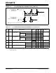
TABLE 15-7: SPI MODE REQUIREMENTS
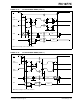
FIGURE 15-15: I
2
C BUS START/STOP BITS TIMING
Param
No.
Symbol Characteristic Min Typ† Max Units Conditions
70* TssL2scH,
TssL2scL
SS
↓ to SCK↓ or SCK↑ input TCY ——ns
71* TscH SCK input high time (Slave mode) T
CY + 20 ——ns
72* TscL SCK input low time (Slave mode) T
CY + 20 ——ns
73* TdiV2scH,
TdiV2scL
Setup time of SDI data input to SCK edge 100 ——ns
74* TscH2diL,
TscL2diL
Hold time of SDI data input to SCK edge 100 ——ns
75* TdoR SDO data output rise time Standard(F)
Extended(LF)
—
—
10
25
25
50
ns
ns
76* TdoF SDO data output fall time — 10 25 ns
77* TssH2doZ SS↑ to SDO output hi-impedance 10 — 50 ns
78* TscR SCK output rise time
(Master mode)
Standard(F)
Extended(LF)
—
—
10
25
25
50
ns
ns
79* TscF SCK output fall time (Master mode) — 10 25 ns
80* TscH2doV,
TscL2doV
SDO data output valid after
SCK edge
Standard(F)
Extended(LF)
—
—
—
—
50
145
ns
ns
81* TdoV2scH,
TdoV2scL
SDO data output setup to SCK edge Tcy ——ns
82* TssL2doV SDO data output valid after SS
↓ edge ——50 ns
83* TscH2ssH,
TscL2ssH
SS
↑ after SCK edge 1.5TCY + 40 ——ns
* These parameters are characterized but not tested.
† Data in "Typ" column is at 5V, 25°C unless otherwise stated. These parameters are for design guidance
only and are not tested.
Note: Refer to Figure 15-3 for load conditions.
91
92
93
SCL
SDA
START
Condition
STOP
Condition
90