
Datasheet


PIC16F72X/PIC16LF72X
DS41341E-page 216 © 2009 Microchip Technology Inc.
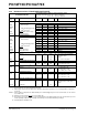
23.3 DC Characteristics: PIC16F72X/PIC16LF72X-I/E (Power-Down)
PIC16LF72X
Standard Operating Conditions (unless otherwise stated)
Operating temperature -40°C ≤ TA ≤ +85°C for industrial
-40°C ≤ T
A ≤ +125°C for extended
PIC16F72X
Standard Operating Conditions (unless otherwise stated)
Operating temperature -40°C ≤ T
A ≤ +85°C for industrial
-40°C ≤ T
A ≤ +125°C for extended
Param
No.
Device Characteristics Min. Typ†
Max.
+85°C
Max.
+125°C
Units
Conditions
V
DD Note
Power-down Base Current (I
PD)
(2)
D020 — 0.02 0.7 3.9 μA 1.8 WDT, BOR, FVR, and T1OSC
disabled, all Peripherals Inactive
— 0.08 1.0 4.3 μA3.0
D020 — 4.3 10.2 17 μA 1.8 WDT, BOR, FVR, and T1OSC
disabled, all Peripherals Inactive
— 5 10.5 18 μA 3.0
— 5.5 11.8 21 μA 5.0
D021 — 0.5 1.7 4.1 μA 1.8 LPWDT Current (Note 1)
— 0.8 2.5 4.8 μA3.0
D021 — 6 13.5 16.4 μA 1.8 LPWDT Current (Note 1)
— 6.5 14.5 16.8 μA 3.0
— 7.5 16 18.7 μA 5.0
D021A — 8.5 14 19 μA 1.8 FVR current (Note 1. Note 3)
— 8.5 14 20 μA3.0
D021A
— 23 44 48 μA 1.8 FVR current (Note 1, Note 3,
Note 5)
— 25 45 55 μA 3.0
— 26 60 70 μA 5.0
D022 — — — — μA 1.8 BOR Current (Note 1, Note 3)
— 7.5 12 22 μA3.0
D022 — — — — μA 1.8 BOR Current (Note 1, Note 3,
Note 5)
— 23 42 49 μA 3.0
— 25 46 50 μA 5.0
D026 — 0.6 2 — μA 1.8 T1OSC Current (Note 1)
—1.83.0 — μA3.0
D026 — 4.5 11.1 — μA 1.8 T1OSC Current (Note 1)
— 6 12.5 — μA 3.0
— 7 13.5 — μA 5.0
† Data in “Typ” column is at 3.0V, 25°C unless otherwise stated. These parameters are for design guidance only and are
not tested.
Note 1: The peripheral current is the sum of the base I
DD or IPD and the additional current consumed when this peripheral is
enabled. The peripheral Δ current can be determined by subtracting the base I
DD or IPD current from this limit. Max
values should be used when calculating total current consumption.
2: The power-down current in Sleep mode does not depend on the oscillator type. Power-down current is measured with
the part in Sleep mode, with all I/O pins in high-impedance state and tied to V
DD.
3: Fixed Voltage Reference is automatically enabled whenever the BOR is enabled
4: A/D oscillator source is F
RC
5: 0.1 μF capacitor on VCAP (RA0).