
Datasheet


PIC16F72X/PIC16LF72X
DS41341E-page 212 © 2009 Microchip Technology Inc.
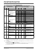
23.1 DC Characteristics: PIC16F72X/PIC16LF72X-I/E (Industrial, Extended)
PIC16LF72X
Standard Operating Conditions (unless otherwise stated)
Operating temperature -40°C ≤ TA ≤ +85°C for industrial
-40°C ≤ T
A ≤ +125°C for extended
PIC16F72X
Standard Operating Conditions (unless otherwise stated)
Operating temperature -40°C ≤ T
A ≤ +85°C for industrial
-40°C ≤ T
A ≤ +125°C for extended
Param.
No.
Sym. Characteristic Min. Typ† Max. Units Conditions
D001 V
DD Supply Voltage
PIC16LF72X 1.8
1.8
2.3
2.5
—
—
—
—
3.6
3.6
3.6
3.6
V
V
V
V
F
OSC ≤ 16 MHz: HFINTOSC, EC
F
OSC ≤ 4MHz
F
OSC ≤ 20 MHz, EC
F
OSC ≤ 20 MHz, HS
D001 PIC16F72X 1.8
1.8
2.3
2.5
—
—
—
—
5.5
5.5
5.5
5.5
V
V
V
V
FOSC ≤ 16 MHz: HFINTOSC, EC
F
OSC ≤ 4 MHz
F
OSC ≤ 20 MHz, EC
F
OSC ≤ 20 MHz, HS
D002* V
DR RAM Data Retention Voltage
(1)
PIC16LF72X 1.5 — — V Device in Sleep mode
D002* PIC16F72X 1.7 — — V Device in Sleep mode
V
POR* Power-on Reset Release Voltage —1.6— V
V
PORR* Power-on Reset Rearm Voltage
PIC16LF72X — 0.8 — V Device in Sleep mode
PIC16F72X — 1.7 — V Device in Sleep mode
D003 V
FVR Fixed Voltage Reference Voltage,
Initial Accuracy
-5.5
-5.5
-5.5
—
—
—
5.5
5.5
5.5
%
%
%
VFVR = 1.024V, VDD ≥ 2.5V
V
FVR = 2.048V, VDD ≥ 2.5V
V
FVR = 4.096V, VDD ≥ 4.75V;
-40 ≤ T
A ≤ 85°C
-6
-6
-6
—
—
—
6
6
6
%
%
%
V
FVR = 1.024V, VDD ≥ 2.5V
V
FVR = 2.048V, VDD ≥ 2.5V
V
FVR = 4.096V, VDD ≥ 4.75V;
-40 ≤ T
A ≤ 125°C
D004* S
VDD VDD Rise Rate to ensure internal
Power-on Reset signal
0.05 — — V/ms See Section 3.2 “Power-on Reset
(POR)” for details.
* These parameters are characterized but not tested.
† Data in “Typ” column is at 3.3V, 25°C unless otherwise stated. These parameters are for design guidance only and are
not tested.
Note 1: This is the limit to which V
DD can be lowered in Sleep mode without losing RAM data.