
Datasheet


PIC16F72X/PIC16LF72X
DS41341E-page 146 © 2009 Microchip Technology Inc.
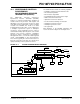
FIGURE 16-2: AUSART RECEIVE BLOCK DIAGRAM
The operation of the AUSART module is controlled
through two registers:
• Transmit Status and Control (TXSTA)
• Receive Status and Control (RCSTA)
These registers are detailed in Register 16-1 and
Register 16-2, respectively.
RX/DT
Pin Buffer
and Control
SPEN
Data
Recovery
CREN OERR
FERR
RSR Register
MSb
LSb
RX9D
RCREG Register
FIFO
Interrupt
RCIF
RCIE
Data Bus
8
Stop
START
(8) 7 1 0
RX9
• • •
SPBRG
FOSC
÷ n
n
+ 1
Multiplier x4 x16 x64
SYNC 100
BRGH x10
Baud Rate Generator