
Datasheet


© 2009 Microchip Technology Inc. DS41341E-page 219
PIC16F72X/PIC16LF72X
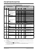
Program Flash Memory
D130 E
P Cell Endurance 100 1k — E/W Temperature during programming:
10°C ≤ T
A ≤ 40°C
D131 V
DD for Read VMIN ——V
Voltage on MCLR
/VPP during
Erase/Program
8.0 — 9.0 V
Temperature during programming:
10°C ≤ TA ≤ 40°C
V
DD for Bulk Erase 2.7 3 — V Temperature during programming:
10°C ≤ T
A ≤ 40°C
D132 V
PEW VDD for Write or Row Erase 2.7 — — V VMIN = Minimum operating voltage
V
MAX = Maximum operating
voltage
I
PPPGM Current on MCLR/VPP during
Erase/Write
——5.0mA
Temperature during programming:
10°C ≤ TA ≤ 40°C
I
DDPGM Current on VDD during Erase/
Write
—
5.0 mA
Temperature during programming:
10°C ≤ T
A ≤ 40°C
D133 T
PEW Erase/Write cycle time — 2.8 ms Temperature during programming:
10°C ≤ T
A ≤ 40°C
D134 T
RETD Characteristic Retention 40 — — Year Provided no other specifications
are violated
V
CAP Capacitor Charging
D135 Charging current — 200 —
μA
D135A Source/sink capability when
charging complete
—0.0—mA
23.4 DC Characteristics: PIC16F72X/PIC16LF72X-I/E (Continued)
DC CHARACTERISTICS
Standard Operating Conditions (unless otherwise stated)
Operating temperature -40°C ≤ TA ≤ +85°C for industrial
-40°C ≤ T
A ≤ +125°C for extended
Param
No.
Sym. Characteristic Min. Typ† Max. Units Conditions
Legend: TBD = To Be Determined
* These parameters are characterized but not tested.
† Data in “Typ” column is at 3.0V, 25°C unless otherwise stated. These parameters are for design guidance only and are
not tested.
Note 1: In RC oscillator configuration, the OSC1/CLKIN pin is a Schmitt Trigger input. It is not recommended to use an external
clock in RC mode.
2: Negative current is defined as current sourced by the pin.
3: The leakage current on the MCLR
pin is strongly dependent on the applied voltage level. The specified levels represent
normal operating conditions. Higher leakage current may be measured at different input voltages.
4: Including OSC2 in CLKOUT mode.